5PB1106PGG Overview
Key Specifications
Package: TSSOP
Mount Type: Surface Mount
Pins: 14
Operating Voltage: 1.8 V
Description
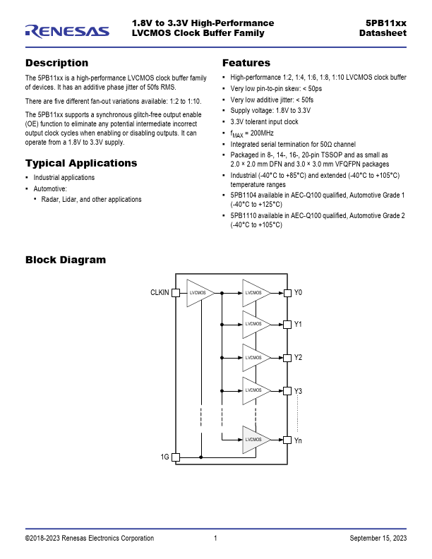
The 5PB11xx is a high-performance LVCMOS clock buffer family of devices. It has an additive phase jitter of 50fs RMS.
| Part | 5PB1106PGG |
|---|---|
| Description | 1.8V to 3.3V High-Performance LVCMOS Clock Buffer |
| Manufacturer | Renesas |
| Size | 1.99 MB |
Package: TSSOP
Mount Type: Surface Mount
Pins: 14
Operating Voltage: 1.8 V
The 5PB11xx is a high-performance LVCMOS clock buffer family of devices. It has an additive phase jitter of 50fs RMS.
| Seller | Inventory | Price Breaks | Buy |
|---|---|---|---|
| Newark | 972 | 1+ : 3.16 USD 10+ : 2.37 USD 25+ : 2.17 USD 50+ : 2.06 USD |
View Offer |
| DigiKey | 0 | 2500+ : 1.75222 USD 5000+ : 1.71547 USD |
View Offer |
| Part Number | Manufacturer | Description |
|---|---|---|
| 5PB1106PGGI | IDT | 1.8V to 3.3V LVCMOS High Performance Clock Buffer |
| 5PB1106PGG | IDT | 1.8V to 3.3V LVCMOS High-Performance Clock Buffer |
| 5PB1106CMGI | IDT | 1.8V to 3.3V LVCMOS High Performance Clock Buffer |
| 5PB1104PGGI | IDT | 1.8V to 3.3V LVCMOS High Performance Clock Buffer |
| 5PB1104PGG | IDT | 1.8V to 3.3V LVCMOS High-Performance Clock Buffer |