Datasheet4U Logo Datasheet4U.com

5PB1214 - TCXO/LVCMOS Clock Buffer

Download the 5PB1214 datasheet PDF. This datasheet also covers the 5PB1203 variant, as both devices belong to the same tcxo/lvcmos clock buffer family and are provided as variant models within a single manufacturer datasheet.

General Description

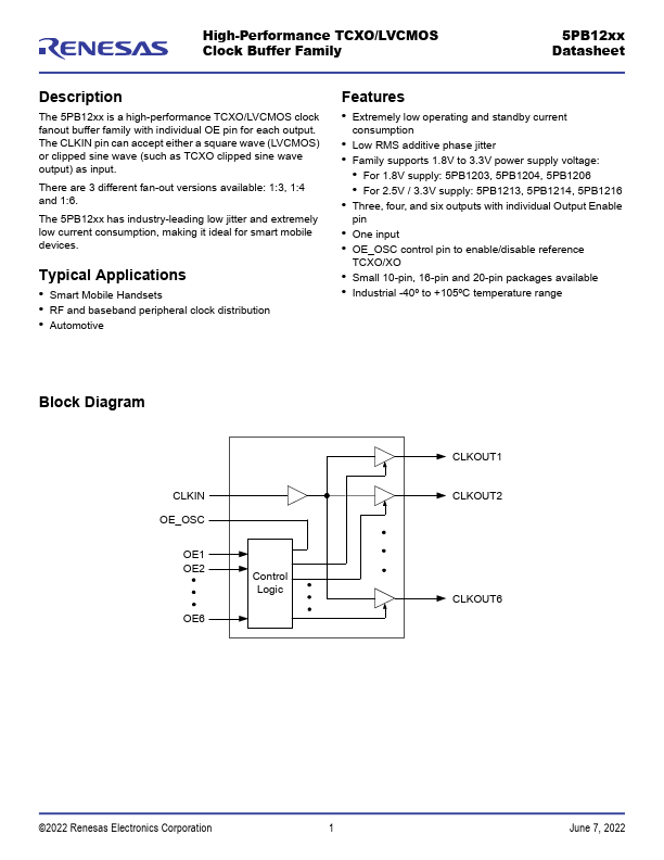
The 5PB12xx is a high-performance TCXO/LVCMOS clock fanout buffer family with individual OE pin for each output.

The CLKIN pin can accept either a square wave (LVCMOS) or clipped sine wave (such as TCXO clipped sine wave output) as input.

Key Features

  • Extremely low operating and standby current consumption.
  • Low RMS additive phase jitter.
  • Family supports 1.8V to 3.3V power supply voltage:.
  • For 1.8V supply: 5PB1203, 5PB1204, 5PB1206.
  • For 2.5V / 3.3V supply: 5PB1213, 5PB1214, 5PB1216.
  • Three, four, and six outputs with individual Output Enable pin.
  • One input.
  • OE_OSC control pin to enable/disable reference TCXO/XO.
  • Small 10-pin, 16-pin and 20-pin packages available.

📥 Download Datasheet

Note: The manufacturer provides a single datasheet file (5PB1203-Renesas.pdf) that lists specifications for multiple related part numbers.

Datasheet Details

Part number 5PB1214
Manufacturer Renesas
File Size 658.82 KB
Description TCXO/LVCMOS Clock Buffer
Datasheet download datasheet 5PB1214 Datasheet

Full PDF Text Transcription (Reference)

The following content is an automatically extracted verbatim text from the original manufacturer datasheet and is provided for reference purposes only.

View original datasheet text
High-Performance TCXO/LVCMOS Clock Buffer Family 5PB12xx Datasheet Description The 5PB12xx is a high-performance TCXO/LVCMOS clock fanout buffer family with individual OE pin for each output. The CLKIN pin can accept either a square wave (LVCMOS) or clipped sine wave (such as TCXO clipped sine wave output) as input. There are 3 different fan-out versions available: 1:3, 1:4 and 1:6. The 5PB12xx has industry-leading low jitter and extremely low current consumption, making it ideal for smart mobile devices. Typical Applications • Smart Mobile Handsets • RF and baseband peripheral clock distribution • Automotive Features • Extremely low operating and standby current consumption • Low RMS additive phase jitter • Family supports 1.8V to 3.3V power supply voltage: • For 1.