621S
Description
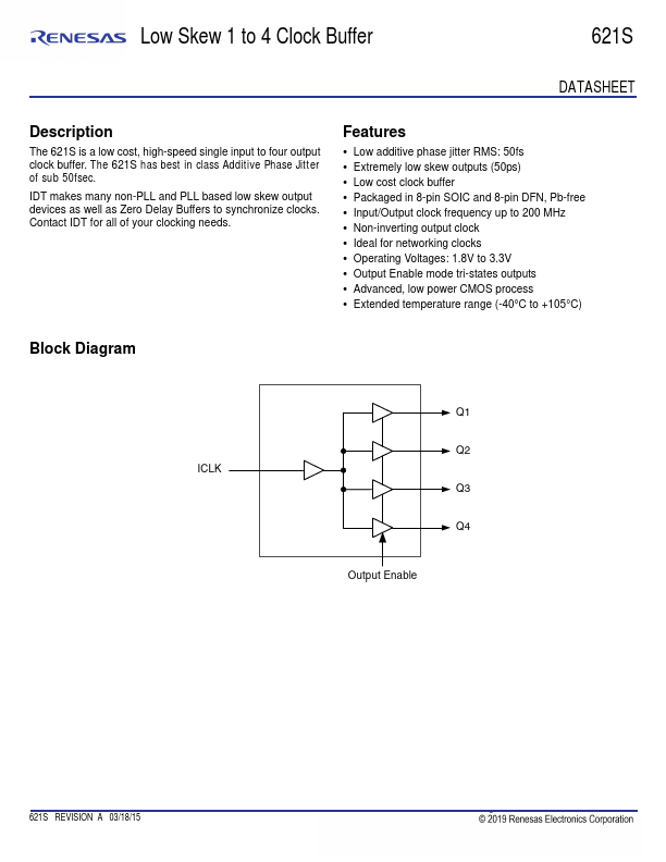
The 621S is a low cost, high-speed single input to four output clock buffer. The 621S has best in class Additive Phase Jitter of sub 50fsec.
IDT makes many non-PLL and PLL based low skew output devices as well as Zero Delay Buffers to synchronize clocks. Contact IDT for all of your clocking needs.
Features
- Low additive phase jitter RMS: 50fs
- Extremely low skew outputs (50ps)
- Low cost clock buffer
- Packaged in 8-pin SOIC and 8-pin DFN, Pb-free
- Input/Output clock frequency up to 200 MHz
- Non-inverting output clock
- Ideal for networking clocks
- Operating Voltages: 1.8V to 3.3V
- Output Enable mode tri-states outputs
- Advanced, low power CMOS process
- Extended temperature range (-40°C to +105°C)
Block Diagram
ICLK
Q1 Q2 Q3 Q4
Output Enable
621S REVISION A 03/18/15
©2015 Integrated Device Technology, Inc.
621S DATASHEET
Pin Assignment
ICLK 1 Q1 2 Q2 3 Q3 4
8 OE 7 VDD 6 GND 5 Q4
8 Pin (150 mil) SOIC
ICLK
Q1
Q2
Q3 4
8 OE 7 VDD 6 GND 5...