Renesas Electronics 83052I
The 83052I is a low skew, 2:1, Single-ended Multiplexer. The 83052I has two selectable single-ended clock inputs and one single-ended clock output. The output has a V pin which may be set at 3.3V, DDO 2.5V, or 1.8V, making the device ideal for use in voltage trans-lation applications.| Part No. | 83052I |
|---|---|
| Datasheet | 83052I Download |
| Manufacturer |  Renesas Electronics |
| Description | Single-Ended Multiplexer |
| Buy | Stock & Price |

GENERAL DESCRIPTION
An output enable pin places the output in a high impedance state which may be useful for testing or debug. The device operates up to 250MHz and is packaged in an 8 TSSOP.FEATURES
● 2:1 single-ended multiplexer● Q nominal output impedance: 15Ω (V = 3.3V) DDO
● Maximum output frequency: 250MHz
● Propagation delay: 2.7ns (maximum), (V = V = 3.3V) DD DDO
● Input skew: 160ps (maximum), (V = V = 3.3V) DD DDO
● Part-to-part skew: 490ps (maximum), (V = V = 3.3V) DD DDO
● Additive phase jitter, RMS at 155.52MHz (12kHz - 20MHz): 0.18ps (typical), (V = V = 3.3V) DD DDO
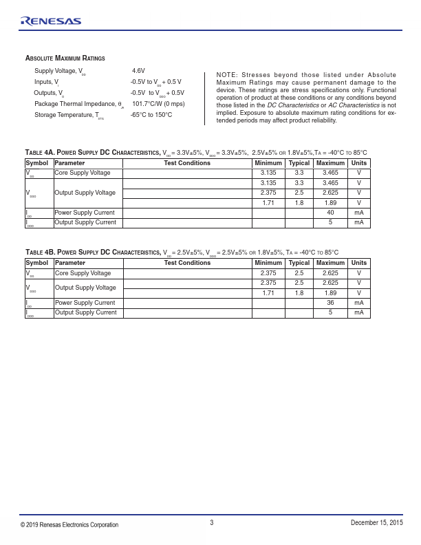
● Operating supply modes: V /V DD DDO 3.3V/3.3V 3.3V/2.5V 3.3V/1.8V 2.5V/2.5V 2.5V/1.8V
● -40°C to 85°C ambient operating temperature
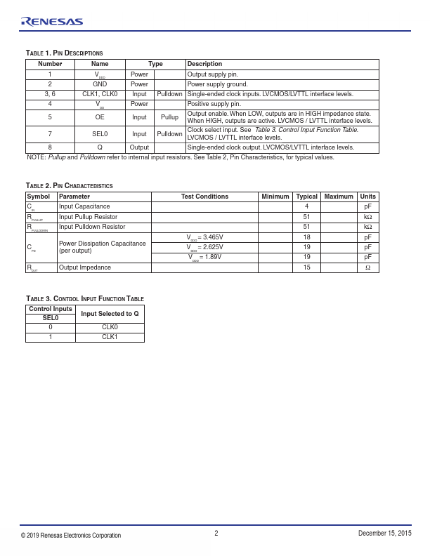
● Available in lead-free (RoHS 6) package BLOCK DIAGRAM CLK0 CLK1 Q SEL0 OE PIN ASSIGNMENT VDDO 1 GND 2 CLK1 3 VDD 4 8Q 7 SEL0 6 CLK0 5 OE 83052I 8-Lead TSSOP 4.40mm x 3.0mm x 0.925mm package body G Package Top View ©2015 Integrated Device Technology, Inc 1 December 15, 2015 83052I Data Sheet TABLE 1.