83115
Description
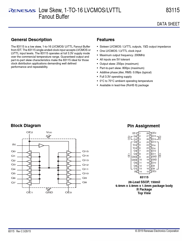
The 83115 is a low skew, 1-to-16 LVCMOS/ LVTTL Fanout Buffer from IDT. The 83115 single-ended clock input accepts LVCMOS or LVTTL input levels. The 83115 operates at full 3.3V supply mode over the mercial temperature range. Guaranteed output and part-to-part skew characteristics make the 83115 ideal for those clock distribution applications demanding well defined performance and repeatability.
Features
- Sixteen LVCMOS / LVTTL outputs, 15 output impedance
- One LVCMOS / LVTTL clock input
- Maximum output frequency: 200MHz
- All inputs are 5V tolerant
- Output skew: 250ps (maximum)
- Part-to-part skew: 800ps (maximum)
- Additive phase jitter, RMS: 0.09ps (typical)
- Full 3.3V operating supply
- 0°C to 70°C ambient operating temperature
- Available in lead-free (Ro HS 6) package
Block Diagram
OE2
VDD 4
Q0 Q1 Q2 Q3 Q4 Q5 Q6 Q7
OE1
4 GND
OE0
Q15 Q14 Q13 Q12 Q11 Q10 Q9 Q8
Pin Assignment
OE2
OE2
OE1 1 Q0 2 Q1 3 Q2 4 VDD 5 VDD 6 Q3 7 Q4 8
GND 9 GND 10
Q5 11 Q6 12...