831752 Overview
Key Specifications
Package: TSSOP
Pins: 16
Operating Voltage: 2.5 V
Max Voltage (typical range): 2.625 V
Description
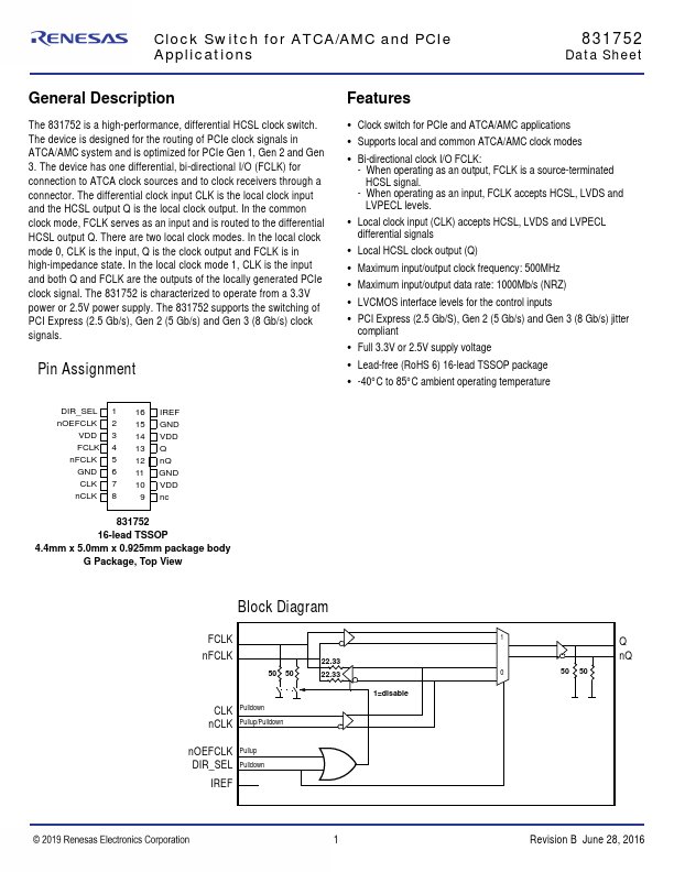
The 831752 is a high-performance, differential HCSL clock switch. The device is designed for the routing of PCIe clock signals in ATCA/AMC system and is optimized for PCIe Gen 1, Gen 2 and Gen 3.
Key Features
- Clock switch for PCIe and ATCA/AMC applications
- Supports local and common ATCA/AMC clock modes
- Bi-directional clock I/O FCLK
- When operating as an output, FCLK is a source-terminated HCSL signal
- When operating as an input, FCLK accepts HCSL, LVDS and LVPECL levels