844N255I
844N255I is NG Crystal-to-LVDS Clock Synthesizer manufactured by Renesas.
Description
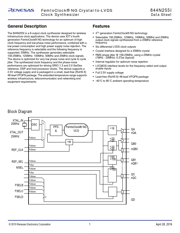
The 844N255I is a 6-output clock synthesizer designed for wireless infrastructure clock applications. The device uses IDT’s fourth generation Femto Clock® NG technology for an optimum of high clock frequency and low phase noise performance, bined with a low power consumption and high power supply noise rejection. The reference frequency is selectable and the following frequency is supported: 25MHz. The synthesizer generates selectable 156.25MHz, 125MHz, 100MHz, 50MHz and 25MHz clock signals. The device is optimized for very low phase noise and cycle to cycle jitter. The synthesized clock frequency and the phase-noise performance are optimized for driving SRIO 1.3 and 2.0 Ser Des reference, DSP and host-processor clocks. The device supports a 2.5V voltage supply and is packaged in a small, lead-free (Ro HS 6) 48-lead VFQFN package. The extended temperature range supports wireless infrastructure, telemunication and networking end equipment requirements.
Features
- 4TH generation Femto Clock® NG technology
- Selectable 156.25MHz, 125MHz, 100MHz, 50MHz and 25MHz output clock signals synthesized from a 25MHz reference frequency
- Six differential LVDS clock outputs
- Crystal interface designed for a 25MHz crystal
- RMS phase jitter @ 156.25MHz, using a 25MHz crystal
(1MHz
- 20MHz): 0.27ps (typical)
- Internal regulator for optimum noise rejection
- LVCMOS interface levels for the frequency select and output enable inputs
- Full 2.5V supply voltage
- Lead-free (Ro HS 6) 48-lead VFQFN package
- -40°C to 85°C ambient operating temperature
Block Diagram
XTAL_IN 25MHz
OSC 0
XTAL_OUT
25MHz
Pulldown
REF_CLK
Pulldown Pulldown
PFD Femto Clock® NG
&
÷M
REF_SEL MSEL
Pulldown Pullup Pulldown
Pullup
Pulldown
Pulldown
FSELB FSELC
Pulldown Pulldown Pulldown
FSELD
÷16
QA n QA
÷÷2250,...