8531-01
Description
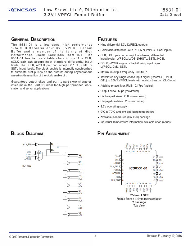
The 8531-01 is a low skew, high performance 1 - t o - 9 D i f fe r e n t i a l - t o - 3.
Key Features
- Nine differential 3.3V LVPECL outputs
- Selectable differential CLK, nCLK or LVPECL clock inputs
- CLK, nCLK pair can accept the following differential input levels: LVPECL, LVDS, LVHSTL, SSTL, HCSL
- PCLK, nPCLK supports the following input types: LVPECL, CML, SSTL
- Maximum output frequency: 500MHz
- Translates any single ended input signal (LVCMOS, LVTTL, GTL) to 3.3V LVPECL levels with resistor bias on nCLK input
- Additive phase jitter, RMS: 0.17ps (typical)
- Output skew: 50ps (maximum)
- Part-to-part skew: 250ps (maximum)
- Propagation delay: 2ns (maximum)