894D115I-04
894D115I-04 is Clock/Data Recovery manufactured by Renesas.
OC-12/STM-4 AND OC-3/STM-1 Clock/Data Recovery Device
Data Sheet
General Description
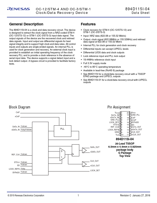
The 894D115I-04 is a clock and data recovery circuit. The device is designed to extract the clock signal from a NRZ-coded STM-4 (OC-12/STS-12) or STM-1 (OC-3/STS-3) input data signal. The output signals of the device are the recovered clock and retimed data signals. Input and output are differential signals for best signal integrity and to support high clock and data rates. All control inputs and outputs are single-ended signals. An internal PLL is used for clock generation and recovery. An external clock input is provided to establish an initial operating frequency of the clock recovery PLL and to provide a clock reference in the absence of serial input data. The device supports a signal detect input and a lock detect output. A bypass circuit is provided to facilitate factory tests.
Features
- Clock recovery for STM-4 (OC-12/STS-12) and
STM-1 (OC-3/STS-3)
- Input: NRZ data (622.08 or 155.52 Mbit/s)
- Output: clock signal (622.08MHz or 155.52MHz) and retimed data signal at 622.08 or 155.52 Mbit/s
- Internal PLL for clock generation and clock recovery
- Differential inputs can accept LVPECL levels
- Differential LVDS data and clock outputs
- Lock reference input and PLL lock output
- 19.44MHz reference clock input
- Full 3.3V supply mode
- -40°C to 85°C operating temperature
- Available in lead-free (Ro HS 6) package
- See 894D115I for a clock/data recovery circuit with a TSSOP
EPAD package and LVPECL outputs
- See 894D115I-01 for a clock/data recovery circuit with LVPECL outputs
Block Diagram
CAP n CAP
DATA_IN Pulldown n DATA_IN Pullup/Pulldown
REF_CLK Pulldown STS12 Pulldown SD Pulldown
LOCK_REFN Pullup BYPASS Pulldown
0 1
DATA_OUT n DATA_OUT
CLK_OUT n CLK_OUT LOCK_DET
Pin Assignment
VDDA DATA_IN n DATA_IN...