97ULPA877A
Description
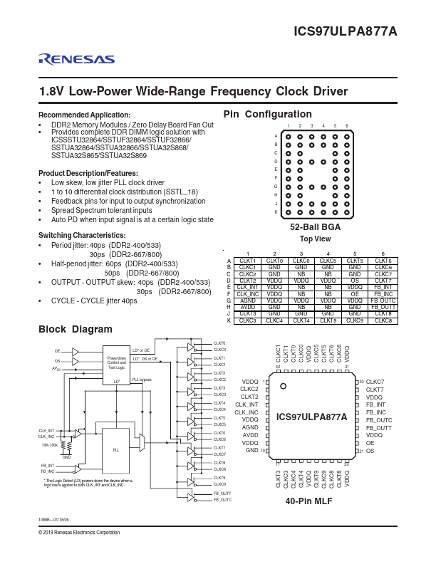
Analog Ground Analog power Clock input with a (10K-100K Ohm) pulldown resistor plentary clock input with a (10K-100K Ohm) pulldown resistor Feedback clock input plementary feedback clock input Feedback clock output plementary feedback clock output Output Enable (Asynchronous) Output Select (tied to GND or VDDQ) Ground Logic and output power Clock outputs plementary clock outputs No ball The PLL clock buffer, ICS97ULPA877A, is designed for a VDDQ of 1.8 V, a AVDD of 1.8 V and differential data input and output levels.
Key Features
- Low skew, low jitter PLL clock driver
- 1 to 10 differential clock distribution (SSTL_18)
- Feedback pins for input to output synchronization
- Spread Spectrum tolerant inputs
- Auto PD when input signal is at a certain logic state
- Period jitter: 40ps (DDR2-400/533)
- Half-period jitter: 60ps (DDR2-400/533)
- CYCLE - CYCLE jitter 40ps