9DB436
9DB436 is 4-Output 3.3V HCSL PCIe Buffer manufactured by Renesas.
4-Output 3.3V HCSL PCIe Buffer
9DB436 Datasheet
Description
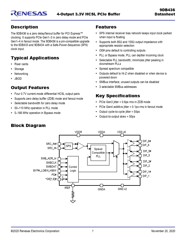
The 9DB436 is a zero delay/fanout buffer for PCI Express™ clocking. It supports PCIe Gen1- 3 in zero delay mode and PCIe Gen1- 4 in fanout mode. The 9DB436 is a pin-patible upgrade to the 9DB433 and 9DB434 with a Safe-Power-Sequence (SPS) clock input.
Typical Applications
- Riser cards
- Storage
- Networking
- JBOD
Output Features
- Four 0.7V current-mode differential HCSL output pairs
- Supports zero delay buffer (ZDB) mode and fanout mode
- Selectable bandwidth for zero delay mode
- 50- 110 MHz operation in PLL mode
- 5- 166 MHz operation in Bypass mode
Features
- SPS internal receiver bias network keeps input clock parked when input is floating
- Supports both 85Ω and 100Ω output impedance with appropriate resistor selection
- OE# pins default to controlling outputs
- PLL or Bypass mode; PLL can dejitter ining clock
- Selectable PLL bandwidth; minimizes jitter peaking in downstream PLLs
- Spread spectrum patible
- Outputs default to Hi-Z when disabled or when device is powered down
- SMBus interface; unused outputs can be disabled
- 3 selectable SMBus addresses
Key Specifications
- PCIe Gen3 jitter < 0.6ps rms in ZDB mode
- PCIe Gen4 additive jitter < 0.1ps rms in fanout mode
- Output cycle-to-cycle jitter < 50ps
- Output-to-output skew <...