Renesas Electronics 9DBL411B
The 9DBL411B is a four output, lower power differential buffer. Each output has its own OE# pin. The device has a maximum operating frequency of 150MHz.| Part No. | 9DBL411B |
|---|---|
| Datasheet | 9DBL411B Download |
| Manufacturer |  Renesas Electronics |
| Description | Low Power Differential Fanout Buffer |
| Buy | Stock & Price |
APPLICATIONS
● PCI-Express Gen1-2-3 or QPI fanout buffer Key Specifications● Output cycle-cycle jitter: < 15ps additive
● Output to output skew: < 50ps
FEATURES
● Low power differential outputs for PCI-Express and QPI clocks● Power down mode when all OE# are high
● Available in commercial (0 to +70°C) and industrial (-40°C to +85°C) temperature ranges
● Available in 20-VFQFPN or 20-TSSOP packages Output
FEATURES
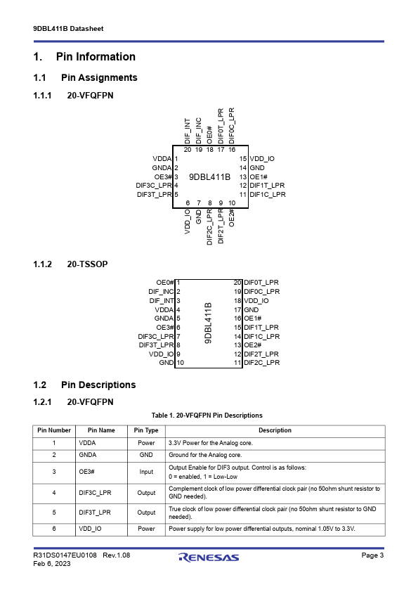
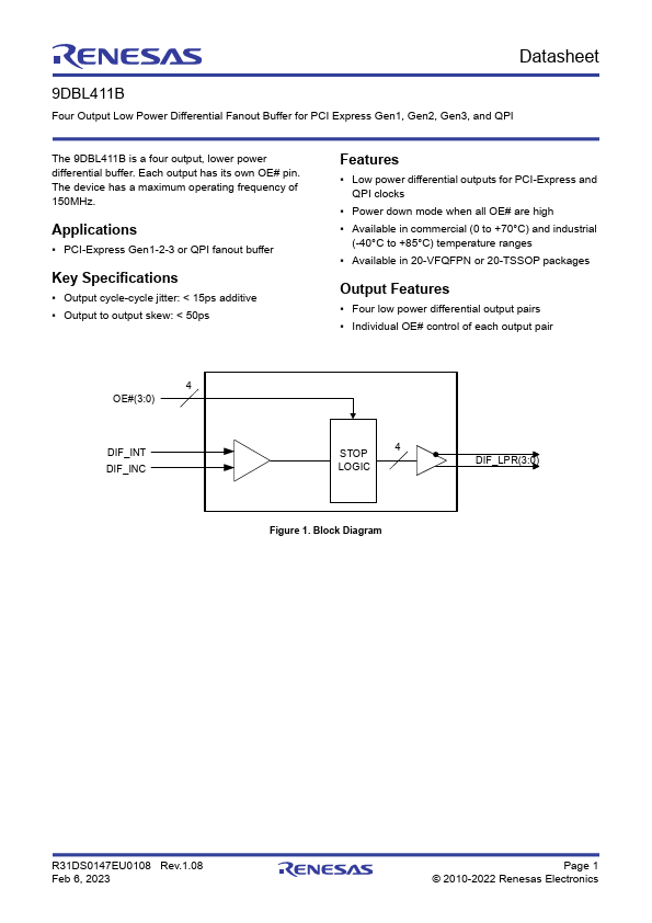
● Four low power differential output pairs● Individual OE# control of each output pair 4 OE#(3:0) DIF_INT DIF_INC STOP 4 LOGIC DIF_LPR(3:0) Figure 1. Block Diagram R31DS0147EU0108 Rev.1.08 Feb 6, 2023 Page 1 © 2010-2022 Renesas Electronics 9DBL411B Datasheet Contents 1. Pin Information . . . . . . . . . . . . . . . . . . . . . . . . . . . . . . . . . . . . . . . . . . . . . . . . . . . . . . . . . . . . . . . . . . . . . . 3 1.1 Pin Assignments . . . . . . . . . . . . . . . . . . . . . . . . . . . . . . . . . . . . . . . . . . . . . . . . . . . . . . . . . . . . . . . . . 3 1.1.1 20-VFQFPN . . . . . . . . . . . . . . . . . . . . . . . . . . . . . . . . . . . . . . . . . . . . . . . . . . . . . . . . . . . . .