9DBV0441 Overview
Key Specifications
Package: 100
Mount Type: Surface Mount
Pins: 32
Operating Voltage: 1.8 V
Description
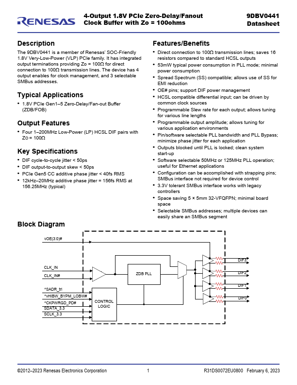
The 9DBV0441 is a member of Renesas’ SOC-Friendly 1.8V Very-Low-Power (VLP) PCIe family. It has integrated output terminations providing Zo = 100 for direct connection to 100 transmission lines.
Key Features
- Four 1–200MHz Low-Power (LP) HCSL DIF pairs with ZO = 100 Key Specifications
- DIF cycle-to-cycle jitter < 50ps
- DIF output-to-output skew < 50ps
- PCIe Gen5 CC additive phase jitter < 40fs RMS
- 12kHz–20MHz additive phase jitter = 156fs RMS at 156.25MHz (typical)