9DBV0531 Overview
Key Specifications
Mount Type: Surface Mount
Pins: 32
Operating Voltage: 1.8 V
Max Voltage (typical range): 1.9 V
Description
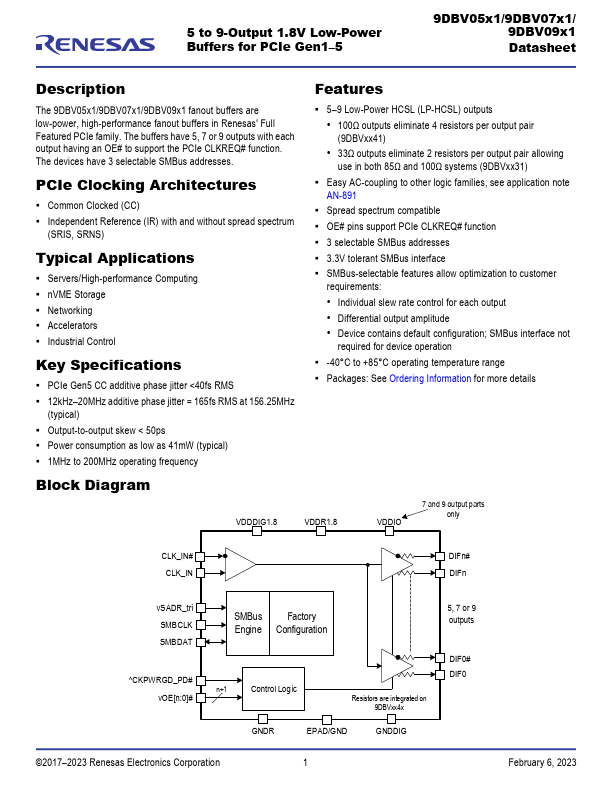
The 9DBV05x1/9DBV07x1/9DBV09x1 fanout buffers are low-power, high-performance fanout buffers in Renesas' Full Featured PCIe family. The buffers have 5, 7 or 9 outputs with each output having an OE# to support the PCIe CLKREQ# function.
Key Features
- 100Ω outputs eliminate 4 resistors per output pair (9DBVxx41)
- Individual slew rate control for each output
- Differential output amplitude
- Device contains default configuration; SMBus interface not required for device operation
- 40°C to +85°C operating temperature range Packages: See