9DBV0641
9DBV0641 is 6-Output 1.8V PCIe Zero-Delay/Fanout Clock Buffer manufactured by Renesas.
6-Output 1.8V PCIe Zero-Delay/Fanout Clock Buffer with Zo = 100ohms
Description
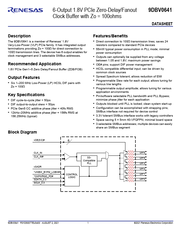
The 9DBV0641 is a member of Renesas’ 1.8V Very-Low-Power (VLP) PCIe family. It has integrated output terminations providing Zo = 100 for direct connection to 100 transmission lines. The device has 6 output enables for clock management and 3 selectable SMBus addresses.
Remended Application
1.8V PCIe Gen1- 5 Zero Delay/Fanout Buffer (ZDB/FOB)
Output Features
- Six 1- 200 MHz Low-Power (LP) HCSL DIF pairs with
Zo = 100
Key Specifications
- DIF cycle-to-cycle jitter < 50ps
- DIF output-to-output skew < 50ps
- PCIe Gen5 CC additive phase jitter < 40fs RMS
- 12kHz- 20MHz additive phase jitter...