9DBV0941
Overview
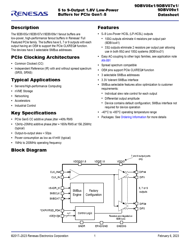
The 9DBV05x1/9DBV07x1/9DBV09x1 fanout buffers are low-power, high-performance fanout buffers in Renesas' Full Featured PCIe family. The buffers have 5, 7 or 9 outputs with each output having an OE# to support the PCIe CLKREQ# function.
- 100Ω outputs eliminate 4 resistors per output pair (9DBVxx41)
- 33Ω outputs eliminate 2 resistors per output pair allowing use in both 85Ω and 100Ω systems (9DBVxx31); Easy AC-coupling to other logic families, see application note AN-891; Spread spectrum compatible; OE# pins support PCIe CLKREQ# function; 3 selectable SMBus addresses; 3.3V tolerant SMBus interface; SMBus-selectable features allow optimization to customer requirements:
- Individual slew rate control for each output
- Differential output amplitude
- Device contains default configuration; SMBus interface not required for device operation; -40°C to +85°C operating temperature range; Packages: See Ordering Information for more details