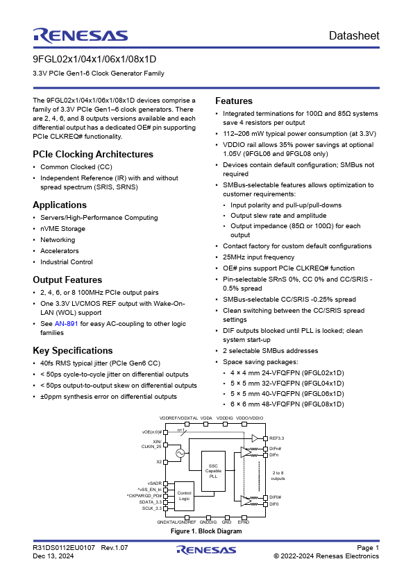
9FGL0651D Overview
Key Specifications
Mount Type: Surface Mount
Pins: 40
Operating Voltage: 3.3 V
Max Voltage (typical range): 3.465 V
Key Features
- Input polarity and pull-up/pull-downs
- Output slew rate and amplitude
| Part | 9FGL0651D |
|---|---|
| Description | 3.3V PCIe Gen1-6 Clock Generator |
| Manufacturer | Renesas |
| Size | 1.39 MB |
Mount Type: Surface Mount
Pins: 40
Operating Voltage: 3.3 V
Max Voltage (typical range): 3.465 V
| Seller | Inventory | Price Breaks | Buy |
|---|---|---|---|
| Renesas | 95 | 1+ : 6.48 USD 10+ : 4.809 USD 25+ : 4.406 USD |
View Offer |
| DigiKey | 95 | 1+ : 6.48 USD 10+ : 4.809 USD 25+ : 4.406 USD |
View Offer |
| Part Number | Manufacturer | Description |
|---|---|---|
| 9FGL0651 | IDT | 6-Output 3.3V PCIe Clock Generator |