9FGV0441
9FGV0441 is 4-OUTPUT VERY LOW POWER PCIE GEN 1-4 CLOCK GENERATOR manufactured by Renesas.
4-OUTPUT VERY LOW POWER PCIE GEN 1- 4 CLOCK GENERATOR
Description
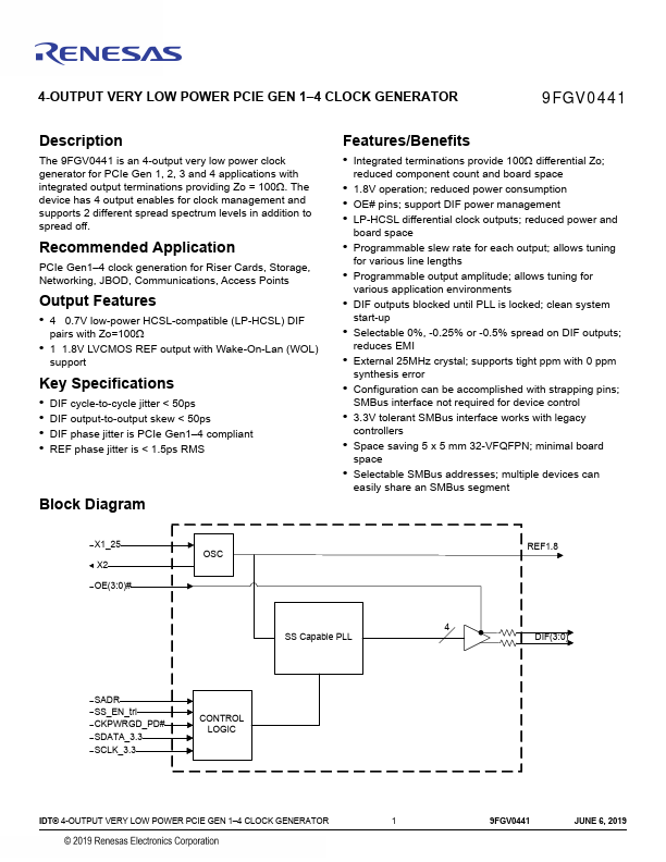
The 9FGV0441 is an 4-output very low power clock generator for PCIe Gen 1, 2, 3 and 4 applications with integrated output terminations providing Zo = 100. The device has 4 output enables for clock management and supports 2 different spread spectrum levels in addition to spread off.
Remended Application
PCIe Gen1- 4 clock generation for Riser Cards, Storage, Networking, JBOD, munications, Access Points
Output Features
- 4 0.7V low-power HCSL-patible (LP-HCSL) DIF pairs with Zo=100
- 1 1.8V LVCMOS REF output with Wake-On-Lan (WOL) support
Key Specifications
- DIF cycle-to-cycle jitter < 50ps
- DIF output-to-output skew < 50ps
- DIF phase jitter is PCIe Gen1- 4 pliant
- REF phase jitter is < 1.5ps RMS
Block Diagram
Features
/Benefits
- Integrated terminations provide 100 differential Zo; reduced ponent count and board space
- 1.8V operation; reduced power consumption
- OE# pins; support DIF power management
- LP-HCSL differential clock outputs; reduced power and board space
- Programmable slew rate for each output; allows tuning for various line lengths
- Programmable output amplitude; allows tuning for various application environments
- DIF outputs blocked until PLL is locked; clean system start-up
- Selectable 0%, -0.25% or -0.5% spread on DIF outputs; reduces EMI
- External 25MHz crystal; supports tight ppm with 0 ppm synthesis error
- Configuration can be acplished with strapping pins;
SMBus interface not required for device control
- 3.3V tolerant SMBus interface works with legacy controllers
- Space saving 5 x 5 mm 32-VFQFPN; minimal board space
- Selectable SMBus addresses; multiple devices can easily share an SMBus...