9FGV1005C Overview
Key Specifications
Package: LGA
Mount Type: Surface Mount
Pins: 16
Operating Voltage: 1.8 V
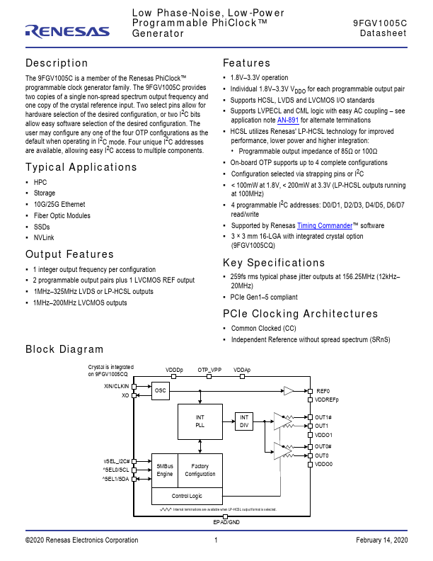
Description
The 9FGV1005C is a member of the Renesas PhiClock™ programmable clock generator family. The 9FGV1005C provides two copies of a single non-spread spectrum output frequency and one copy of the crystal reference input.