9FGV1005C
9FGV1005C is Programmable PhiClock Generators manufactured by Renesas.
- Part of the 9FGV1001C comparator family.
- Part of the 9FGV1001C comparator family.
Low Phase-Noise, Low-Power Programmable Phi Clock™ Generators
9FGV1001C / 9FGV1005C Datasheet
Description
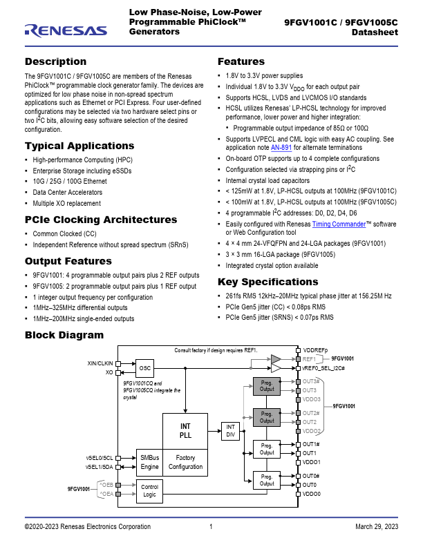
The 9FGV1001C / 9FGV1005C are members of the Renesas Phi Clock™ programmable clock generator family. The devices are optimized for low phase noise in non-spread spectrum applications such as Ethernet or PCI Express. Four user-defined configurations may be selected via two hardware select pins or two I2C bits, allowing easy software selection of the desired configuration.
Typical Applications
- High-performance puting (HPC)
- Enterprise Storage including e SSDs
- 10G / 25G / 100G Ethernet
- Data Center Accelerators
- Multiple XO replacement
PCIe Clocking Architectures
- mon Clocked (CC)
- Independent Reference without spread spectrum (SRn S)
Output Features
- 9FGV1001: 4 programmable output pairs plus 2 REF outputs
- 9FGV1005: 2 programmable output pairs plus 1 REF output
- 1 integer output frequency per configuration
- 1MHz- 325MHz differential outputs
- 1MHz- 200MHz single-ended outputs
Features
- 1.8V to 3.3V power supplies
- Individual 1.8V to 3.3V VDDO for each output pair
- Supports HCSL, LVDS and LVCMOS I/O standards
- HCSL utilizes Renesas’ LP-HCSL technology for improved performance, lower power and higher integration:
- Programmable output impedance of 85Ω or 100Ω
- Supports LVPECL and CML logic with easy AC coupling. See application note AN-891 for alternate terminations
- On-board OTP supports up to 4 plete configurations
- Configuration selected via strapping pins or I2C
- Internal crystal load capacitors
- < 125m W at 1.8V, LP-HCSL outputs at 100MHz...