9SBV0802
Description
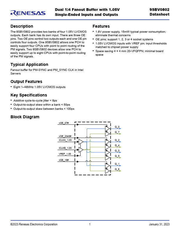
The 9SBV0802 provides two banks of four 1.05V LVCMOS outputs. Each bank has its own input. There are three OE pins. Two OE pins control two outputs each and one OE pin controls four outputs. One 9SBV0802 allows one PCH to easily support four CPUs with point to point routing of the PM signals. Two 9SBV0802 devices allow one PCH to easily support up to eight CPUs with point-to-point routing of the PM signals.
Typical Application
Fanout buffer for PM-SYNC and PM_SYNC CLK in Intel Servers
Output Features
- Eight 1- 48MHz 1.05V LVCMOS outputs
Key Specifications
- Additive cycle-to-cycle jitter < 8ps
- Output-to-output skew within a bank < 50ps
- Output-to-output skew between banks < 100ps
Block Diagram v OE_07# v OE_2345# ICLKA_1.05
ICLKB_1.05 VREF_1.05 v OE_16#
Features
- 1.8V power supply, 15m W typical power consumption; eliminate thermal concerns
- OE pins; support 1, 2, 3 or 4 socket systems
- 1.05V LVCMOS inputs with VREF pin; input thresholds matched to chipset power...