EL7155
EL7155 is High Performance Pin Driver manufactured by Renesas.
Features
- Clocking speeds up to 40MHz
- 15ns tr/tf at 2000p F CLOAD
- 0.5ns rise and fall times mismatch
- 0.5ns t ON-t OFF prop delay mismatch
- 3.5p F typical input capacitance
- 3.5A peak drive
- Low ON-resistance of 3.5Ω
- High capacitive drive capability
- Operates from 4.5V up to 16.5V
- Pb-free (Ro HS pliant)
Applications
- ATE/burn-in testers
- Level shifting
- IGBT drivers
- CCD drivers
FN7279 Rev 3.00 October 24, 2014
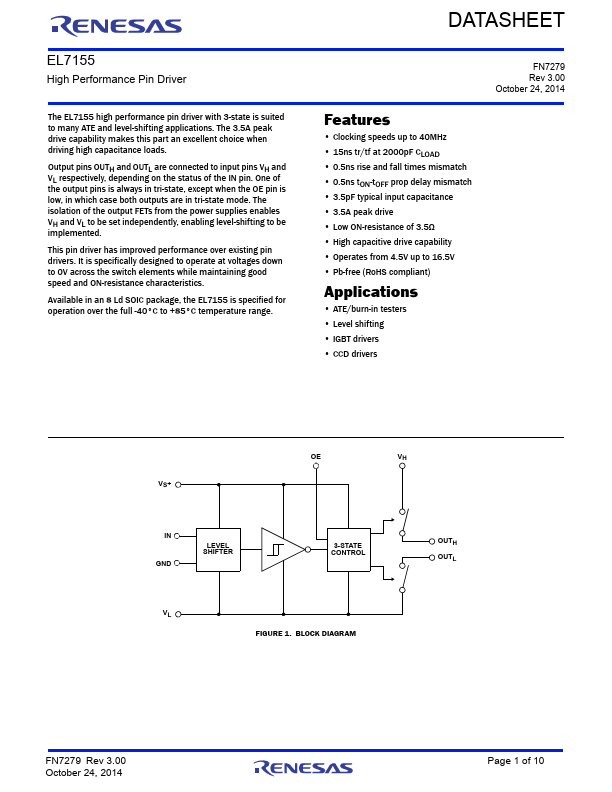
VS+
IN GND
LEVEL SHIFTER
3-STATE CONTROL
OUTH OUTL
FIGURE 1. BLOCK DIAGRAM
FN7279 Rev 3.00 October 24, 2014
Page 1 of 10
Pin Configuration
EL7155 (8 LD SOIC) TOP VIEW
VS+ 1
OE 2
IN 3
8 VH 7 OUTH 6 OUTL
GND...