HD74HC534
HD74HC534 is Octal D-type Flip-Flops manufactured by Renesas.
- Part of the HD74HC374 comparator family.
- Part of the HD74HC374 comparator family.
Description
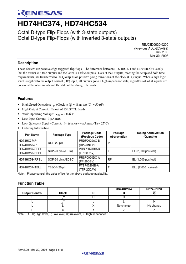
These devices are positive edge triggered flip-flops. The difference between HD74HC374 and HD74HC534 is only that the former is a true outputs and the latter is a false outputs. Data at the D inputs, meeting the setup and hold time requirements, are transferred to the Q outputs on positive going transitions of the clock (CK) input. When a high logic level is applied to the output control (OC) input, all outputs go to a high impedance state, regardless of what signals are present at the other inputs and the state of the storage elements.
Features
- High Speed Operation: tpd (Clock to Q) = 18 ns typ (CL = 50 p F)
- High Output Current: Fanout of 15 LSTTL Loads
- Wide Operating Voltage: VCC = 2 to 6 V
- Low Input Current: 1 µA max
- Low Quiescent Supply Current: ICC (static) = 4 µA max (Ta = 25°C)
- Ordering Information
Part Name
Package Type
Package Code (Previous Code)
Package Abbreviation
HD74HC374P HD74HC534P
DILP-20 pin
PRDP0020AC-B (DP-20NEV)
HD74HC374FPEL HD74HC534FPEL
SOP-20 pin (JEITA)
PRSP0020DD-B (FP-20DAV)
HD74HC534RPEL
SOP-20 pin (JEDEC)
PRSP0020DC-A (FP-20DBV)
HD74HC374TELL TSSOP-20 pin
PTSP0020JB-A (TTP-20DAV)
Note: Please consult the sales office for the above package availability.
Taping Abbreviation (Quantity)
- EL (2,000 pcs/reel)
EL (1,000 pcs/reel)
ELL (2,000 pcs/reel)
Function Table
Output...


