HD74LV595A
HD74LV595A is 8-bit Shift Registers manufactured by Renesas.
Description
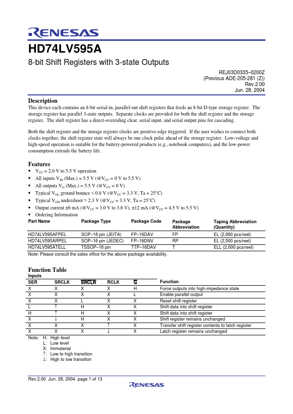
This device each contains an 8-bit serial-in, parallel-out shift registers that feeds an 8-bit D-type storage register. The storage register has parallel 3-state outputs. Separate clocks are provided for both the shift register and the storage register. The shift register has a direct-overriding clear, serial input, and serial output pins for cascading.
Both the shift register and the storage register clocks are positive-edge triggered. If the user wishes to connect both clocks together, the shift register state will always be one clock pulse ahead of the storage register. Low-voltage and high-speed operation is suitable for the battery-powered products (e.g., notebook puters), and the low-power consumption extends the battery life.
Features
- VCC = 2.0 V to 5.5 V operation
- All inputs VIH (Max.) = 5.5 V (@VCC = 0 V to 5.5 V)
- All...