Datasheet Summary
Dual D- type Flip Flops with Preset and Clear
REJ03D0312- 0300Z (Previous ADE-205-244A (Z))
Rev.3.00 Jun. 02, 2004
Description
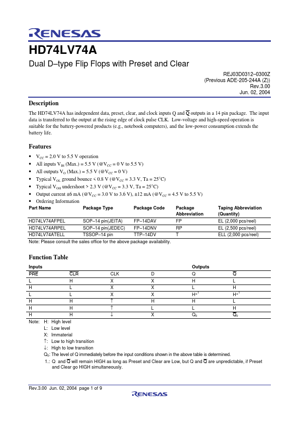
The HD74LV74A has independent data, preset, clear, and clock inputs Q and Q outputs in a 14 pin package. The input data is transferred to the output at the rising edge of clock pulse CLK. Low-voltage and high-speed operation is suitable for the battery-powered products (e.g., notebook puters), and the low-power consumption extends the battery life.
Features
- VCC = 2.0 V to 5.5 V operation
- All inputs VIH (Max.) = 5.5 V (@VCC = 0 V to 5.5 V)
- All outputs VO (Max.) = 5.5 V (@VCC = 0 V)
- Typical VOL ground bounce < 0.8 V (@VCC = 3.3 V, Ta = 25°C)
-...