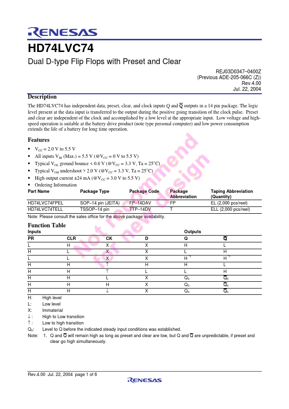
HD74LVC74 Description
REJ03D0347 0400Z (Previous ADE-205-066C (Z)) Rev.4.00 Jul. 22, 2004 The HD74LVC74 has independent data, preset, clear, and clock inputs Q and Q outputs in a 14 pin package. The logic level present at the data input is transferred to the output during the positive going transition of the clock pulse.
HD74LVC74 Key Features
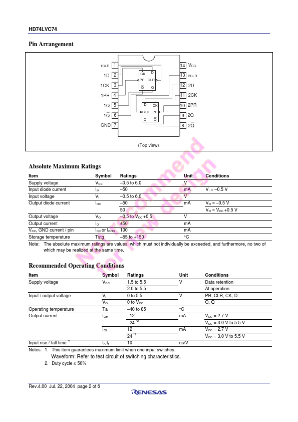
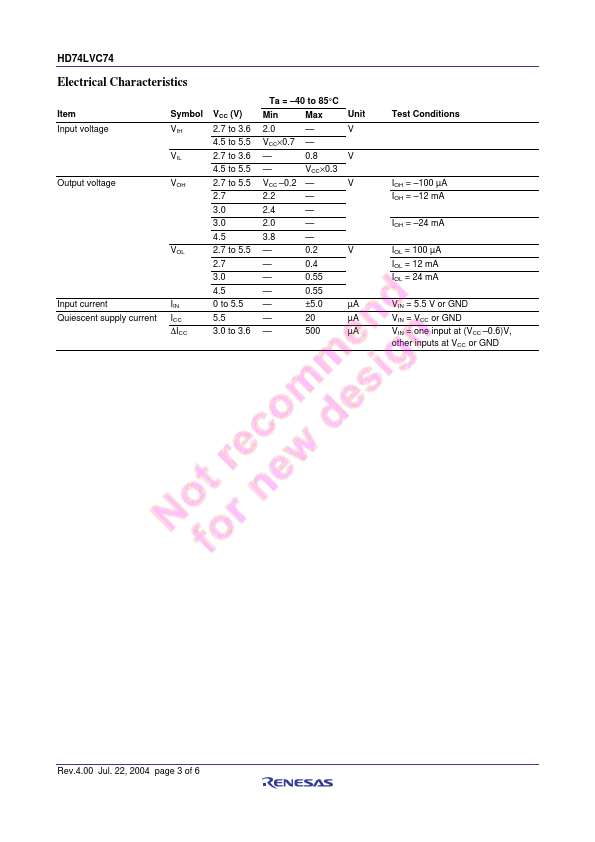
- VCC = 2.0 V to 5.5 V
- All inputs VIH (Max.) = 5.5 V (@VCC = 0 V to 5.5 V)
- Typical VOL ground bounce < 0.8 V (@VCC = 3.3 V, Ta = 25°C)
- Typical VOH undershoot > 2.0 V (@VCC = 3.3 V, Ta = 25°C)
- High output current ±24 mA (@VCC = 3.0 V to 5.5 V)
- Ordering Information