ICS9248-77
Description
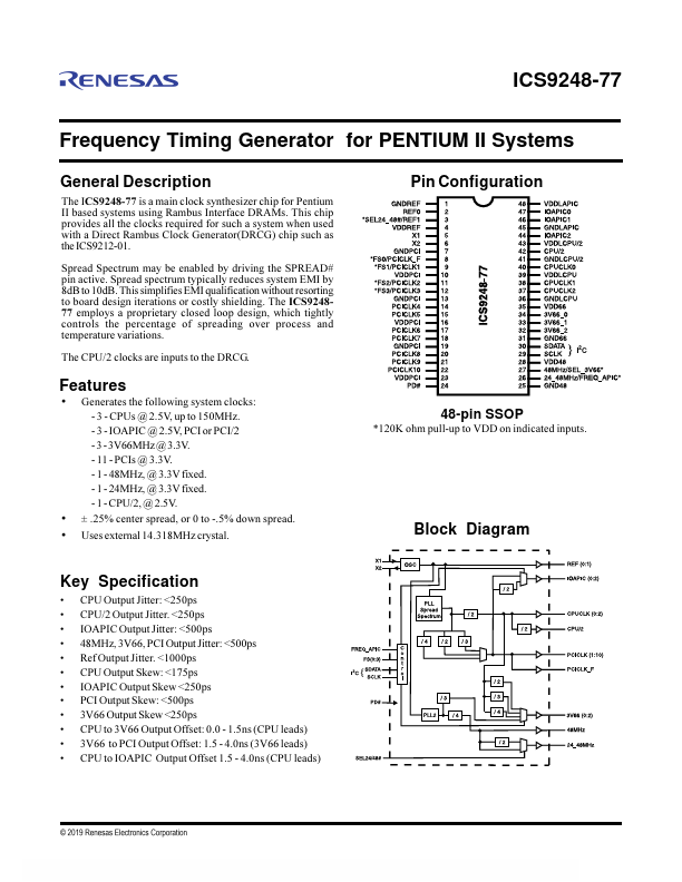
The ICS9248-77 is a main clock synthesizer chip for Pentium II based systems using Rambus Interface DRAMs. This chip provides all the clocks required for such a system when used with a Direct Rambus Clock Generator(DRCG) chip such as the ICS9212-01.
Spread Spectrum may be enabled by driving the SPREAD# pin active. Spread spectrum typically reduces system EMI by 8d B to 10d B. This simplifies EMI qualification without resorting to board design iterations or costly shielding. The ICS924877 employs a proprietary closed loop design, which tightly controls the percentage of spreading over process and temperature variations.
The CPU/2 clocks are inputs to the DRCG.
Features
Generates the following system clocks:
- 3
- CPUs @ 2.5V, up to 150MHz.
- 3
- IOAPIC @ 2.5V, PCI or PCI/2
- 3
- 3V66MHz @ 3.3V.
- 11
- PCIs @ 3.3V.
- 1
- 48MHz, @ 3.3V fixed.
- 1
- 24MHz, @ 3.3V fixed.
- 1
- CPU/2, @ 2.5V.
± .25% center spread, or 0 to -.5% down spread. Uses external 14.318MHz...