ICS951601
ICS951601 is General Purpose Frequency Timing Generator manufactured by Renesas.
Preliminary Product Preview
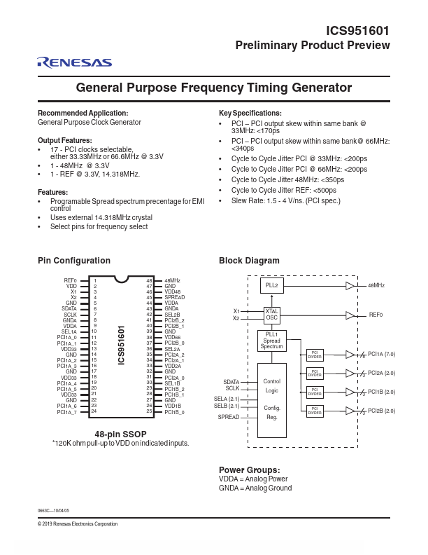
General Purpose Frequency Timing Generator
Remended Application: General Purpose Clock Generator
Output Features
:
- 17
- PCI clocks selectable, either 33.33MHz or 66.6MHz @ 3.3V
- 1
- 48MHz @ 3.3V
- 1
- REF @ 3.3V, 14.318MHz.
Features
:
- Programable Spread spectrum precentage for EMI control
- Uses external 14.318MHz crystal
- Select pins for frequency select
Key Specifications:
- PCI
- PCI output skew within same bank @
33MHz: <170ps
- PCI
- PCI output skew within same bank@ 66MHz: <340ps
- Cycle to Cycle Jitter PCI @ 33MHz: <200ps
- Cycle to Cycle Jitter PCI @ 66MHz: <200ps
- Cycle to Cycle Jitter 48MHz: <350ps
- Cycle to Cycle Jitter REF:...