ICSSSTVA16859C
ICSSSTVA16859C is DDR 13-Bit to 26-Bit Registered Buffer manufactured by Renesas.
DDR 13-Bit to 26-Bit Registered Buffer
Remended Applications:
- DDR Memory Modules:
- DDRI (PC1600, PC2100)
- DDR333 (PC2700)
- DDRI-400 (PC3200)
- Provides plete DDR DIMM solution with ICS93V857 or ICS95V857
- SSTL_2 patible data registers
Product Features
:
- Differential clock signals
- Meets SSTL_2 signal data
- Supports SSTL_2 class I specifications on outputs
- Low-voltage operation
- VDD = 2.3V to 2.7V
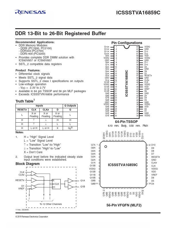
- Available in 64 pin TSSOP and 56 pin MLF packages
- Exceeds ICSSSTVN16859 performance
Truth Table1
RESET#
Notes:
Inputs
CLK#
X or X or Floating Floating
↑↓
↑↓
L or H L or H
Q Outputs
X or Floating
X Q0(2)
1. H = "High" Signal Level L = "Low" Signal Level ↑ = Transition "Low"-to-"High" ↓ = Transition "High"-to-"Low" X = Don't...