IDT49FCT3805B
Overview
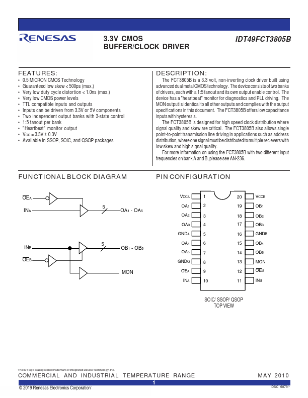
The FCT3805B is a 3.3 volt, non-inverting clock driver built using advanced dual metal CMOS technology. The device consists of two banks of drivers, each with a 1:5 fanout and its own output enable control.
- 0.5 MICRON CMOS Technology
- Guaranteed low skew < 500ps (max.)
- Very low duty cycle distortion < 1.0ns (max.)
- Very low CMOS power levels
- TTL compatible inputs and outputs
- Inputs can be driven from 3.3V or 5V components
- Two independent output banks with 3-state control
- 1:5 fanout per bank
- "Heartbeat" monitor output
- VCC = 3.3V ± 0.3V