IDT5V41067A Overview
Key Specifications
Package: TSSOP
Mount Type: Surface Mount
Max Frequency: 200 MHz
Max Operating Temp: 70 °C
Description
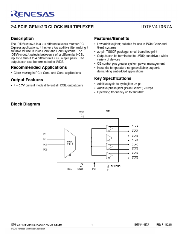
The IDT5V41067A is a 2:4 differential clock mux for PCI Express applications. It has very low additive jitter making it suitable for use in PCIe Gen2 and Gen3 systems.
Key Features
- 4 – 0.7V current mode differential HCSL output pairs Features/Benefits
- Low additive jitter; suitable for use in PCIe Gen2 and Gen3 systems
- 20-pin TSSOP package; small board footprint
- Outputs can be terminated to LVDS; can drive a wider variety of devices
- OE control pin; greater system power management