IDT72V73263
IDT72V73263 is 3.3 VOLT TIME SLOT INTERCHANGE DIGITAL SWITCH manufactured by Renesas.
3.3 VOLT TIME SLOT INTERCHANGE DIGITAL SWITCH WITH RATE MATCHING 16,384 X 16,384 CHANNELS
Features
:
- Up to 64 serial input and output streams
- Maximum 16,384 x 16,384 channel non-blocking switching
- Accepts data streams at 2.048Mb/s, 4.096Mb/s, 8.192Mb/s,
16.384Mb/s or 32.768Mb/s
- Rate matching capability: rate selectable on both RX and TX in eight groups of 8 streams
- Optional Output Enable Indication Pins for external driver
High-Z control
- Per-channel Variable Delay Mode for low-latency applications
- Per-channel Constant Delay Mode for frame integrity applications
- Enhanced Block programming capabilities
- TX/RX Internal Bypass
- Automatic identification of ST-BUS and GCI serial streams
- Per-stream frame delay offset programming
- Per-channel High-Impedance output control
- Per-channel processor mode to allow microprocessor writes to TX streams
- Bit Error Rate Testing (BERT) for testing
- Direct microprocessor access to all internal memories
- Selectable Synchronous and Asynchronous Microprocessor bus timing modes
- IEEE-1149.1 (JTAG) Test Port
- Available in 208-pin (17mm x 17mm) Plastic Ball Grid Array (PBGA)
- Operating Temperature Range -40°C to +85°C
DESCRIPTION:
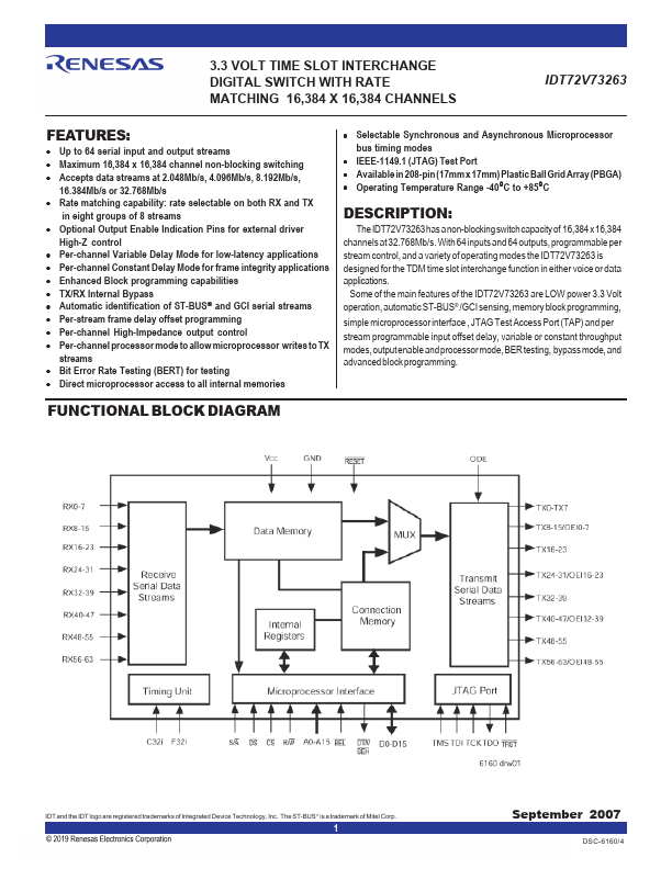
The IDT72V73263 has a non-blocking switch capacity of 16,384 x 16,384 channels at 32.768Mb/s. With 64 inputs and 64 outputs, programmable per stream control, and a variety of operating modes the IDT72V73263 is designed for the TDM time slot interchange function in either voice or data applications.
Some of the main Features of the IDT72V73263 are LOW power 3.3 Volt operation, automatic ST-BUS® /GCI sensing, memory block programming, simple microprocessor interface , JTAG Test Access Port (TAP) and per stream programmable input offset delay, variable or constant throughput modes, output enable and processor mode, BER testing, bypass mode, and advanced block programming.
FUNCTIONAL BLOCK DIAGRAM
IDT and the IDT logo are registered trademarks of Integrated Device...