IDTCV123
IDTCV123 is PROGRAMMABLE CLOCK manufactured by Renesas.
FEATURES
:
- One high precision PLL for CPU, with SSC and N programmable
- One high precision PLL for SRC/PCI/SATA, SSC and N programmable
- One high precision PLL for 96MHz/48MHz
- Band-gap circuit for differential outputs
- Supports spread spectrum modulation, down spread 0.5%
- Supports SMBus block read/write, index read/write
- Selectable output strength for REF
- Allows for CPU frequency to change to a higher frequency for maximum system puting power
- Available in SSOP package
OUTPUTS:
- 2- 0.7V current
- mode differential CPU CLK pair
- 8- 0.7V current
- mode differential SRC CLK pair, one dedicated for SATA
- One CPU_ITP/SRC selectable CLK pair
- 8- PCI, 3 free running, 33.3MHz
- 1- 96MHz,1- 48MHz
- 2- REF
DESCRIPTION
:
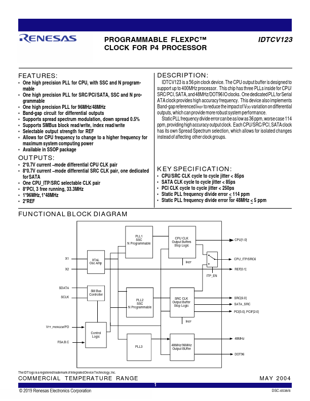
IDTCV123 is a 56 pin clock device. The CPU output buffer is designed to support up to 400MHz processor. This chip has three PLLs inside for CPU/ SRC/PCI, SATA, and 48MHz/DOT96 IO clocks. One dedicated PLL for Serial ATA clock provides high accuracy frequency. This device also implements Band-gap referenced IREF to reduce the impact of VDD variation on differential outputs, which can provide more robust system performance.
Static PLL frequency divide error can be as low as 36 ppm, worse case 114 ppm, providing high accuracy output clock. Each CPU/SRC/PCI, SATA clock has its own Spread Spectrum selection, which allows for isolated changes instead of affecting other clock groups.
KEY SPECIFICATION:
- CPU/SRC CLK cycle to cycle jitter < 85ps
- SATA CLK cycle to cycle jitter < 85ps
- PCI CLK cycle to cycle jitter < 250ps
- Static PLL frequency divide error < 114 ppm
- Static PLL frequency divide error for 48MHz < 5 ppm
FUNCTIONAL BLOCK DIAGRAM
X1 X2
SDATA SCLK
XTAL Osc Amp
SM Bus Controller
VTT_PWRGD#/PD FSA.B.C
Control Logic
PLL1 SSC N Programmable
CPU CLK Output Buffers
Stop...