IDTF0480NBGI
Overview
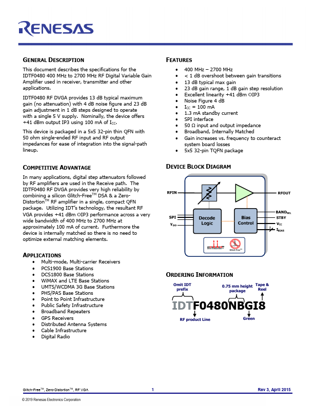
This document describes the specifications for the IDTF0480 400 MHz to 2700 MHz RF Digital Variable Gain Amplifier used in receiver, transmitter and other applications. IDTF0480 RF DVGA provides 13 dB typical maximum gain (no attenuation) with 4 dB noise.
- 400 MHz - 2700 MHz
- < 1 dB overshoot between gain transitions
- 13 dB typical max gain
- 23 dB gain range, 1 dB gain step resolution
- Excellent linearity +41 dBm OIP3
- Noise Figure 4 dB
- ICC = 100 mA
- 1.3 mA standby current
- SPI interface
- 50 Ω input and output impedance