ISL23425
ISL23425 is Low Voltage Digitally Controlled Potentiometer manufactured by Renesas.
Dual, 256-Tap, Low Voltage Digitally Controlled Potentiometer (XDCP™)
FN7873 Rev 1.00 September 11, 2015
The ISL23425 is a volatile, low voltage, low noise, low power, 256-tap, dual digitally controlled potentiometer (DCP) with an SPI Bus™ interface. It integrates two DCP cores, wiper switches and control logic on a monolithic CMOS integrated circuit.
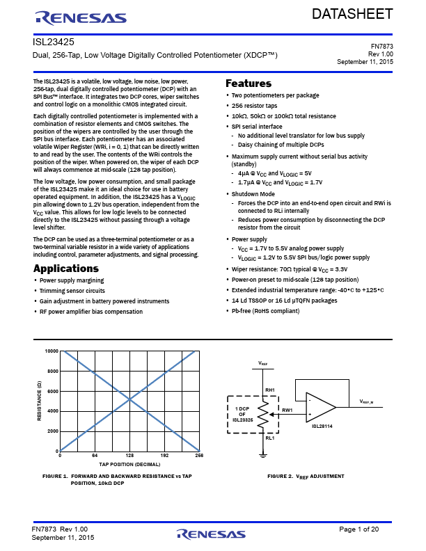
Each digitally controlled potentiometer is implemented with a bination of resistor elements and CMOS switches. The position of the wipers are controlled by the user through the SPI bus interface. Each potentiometer has an associated volatile Wiper Register (WRi, i = 0, 1) that can be directly written to and read by the user. The contents of the WRi controls the position of the wiper. When powered on, the wiper of each DCP will always mence at mid-scale (128 tap position).
The low voltage, low power consumption, and small package of the ISL23425 make it an ideal choice for use in battery operated equipment. In addition, the ISL23425 has a VLOGIC pin allowing down to 1.2V bus operation, independent from the VCC value. This allows for low logic levels to be connected directly to the ISL23425 without passing through a voltage level shifter.
The DCP can be used as a three-terminal potentiometer or as a two-terminal variable resistor in a wide variety of applications including control, parameter adjustments, and signal processing.
Applications
- Power supply margining
- Trimming sensor circuits
- Gain adjustment in battery powered instruments
- RF power amplifier bias pensation
Features
- Two potentiometers per package
- 256 resistor taps
- 10k 50kor 100k total resistance
- SPI serial interface
- No additional level translator for low bus supply
- Daisy Chaining of multiple DCPs
- Maximum supply current without serial bus activity (standby)
- 4µA @ VCC and VLOGIC = 5V
- 1.7µA @ VCC and VLOGIC = 1.7V
- Shutdown Mode
- Forces the DCP into an end-to-end open circuit and RWi is connected to...