ISL9111A
ISL9111A is High Efficiency Synchronous Boost Converter manufactured by Renesas.
- Part of the ISL9111 comparator family.
- Part of the ISL9111 comparator family.
feature
, which will internally shut off at 0.7V protecting a rechargeable battery. The ISL9111A has this feature disabled to maximize the usable life of a non-rechargeable single cell battery. The parts are available in fixed 3.0V, 3.3V and 5.0V output voltage versions or an adjustable output voltage version (ADJ). The fixed output voltage version also provides a FAULT pin for fault condition monitoring. The ISL9111 and ISL9111A are available in a 6 Ld SOT-23 package.
Features
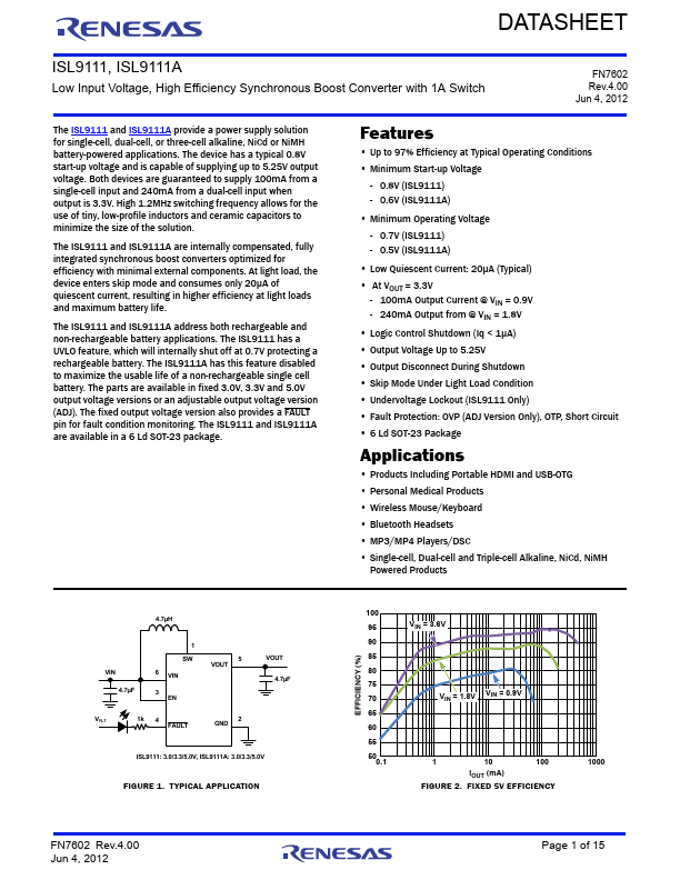
- Up to 97% Efficiency at Typical Operating Conditions
- Minimum Start-up Voltage
- 0.8V (ISL9111)
- 0.6V (ISL9111A)
- Minimum Operating Voltage
- 0.7V (ISL9111)
- 0.5V (ISL9111A)
- Low Quiescent Current: 20μA (Typical)
- At VOUT = 3.3V
- 100m A Output Current @ VIN = 0.9V
- 240m A Output from @ VIN = 1.8V
- Logic Control Shutdown (Iq < 1µA)
- Output Voltage Up to 5.25V
- Output Disconnect During Shutdown
- Skip Mode Under Light Load Condition
- Undervoltage Lockout (ISL9111 Only)
- Fault Protection: OVP (ADJ Version Only), OTP, Short Circuit
- 6 Ld SOT-23 Package
Applications
- Products Including Portable HDMI and USB-OTG
- Personal Medical Products
- Wireless Mouse/Keyboard
- Bluetooth Headsets
- MP3/MP4 Players/DSC
- Single-cell, Dual-cell and Triple-cell Alkaline, Ni Cd, Ni MH
Powered Products
4.7µH
VIN 4.7µF
1 SW 6 VIN
3 EN
VFLT
1k 4
FAULT
5 VOUT
GND 2
VOUT 4.7µF
ISL9111: 3.0/3.3/5.0V, ISL9111A:...