Datasheet4U Logo Datasheet4U.com

ISLA212P50 - 500MSPS ADC

Description

- 72 Ld QFN, LVDS Mode PIN NUMBER 1, 2, 17, 57, 58, 59, 60 6, 13, 19, 20, 21, 70, 71, 72 5, 7, 12, 14 27, 32, 62 26, 45, 61, 65 3 4 8, 9 LVDS PIN NAME DNC AVDD AVSS OVDD OVSS NAPSLP VCM VINN LVDS PIN FUNCTION Do Not Connect 1.8V Analog Supply Analog Ground 1.8V Output Supply Output Ground Tri-Le

Features

  • Automatic fine interleave correction calibration.
  • Single supply 1.8V operation.
  • Clock duty cycle stabilizer.
  • 75f clock jitter.
  • 700MHz bandwidth.
  • Programmable built-in test patterns.
  • Multi-ADC support - SPI programmable fine gain and offset control - Support for multiple ADC synchronization - Optimized output timing.
  • Nap and sleep modes - 200µs sleep wake-up time.
  • Data output clock.
  • DDR LVDS-compatible or L.

📥 Download Datasheet

Datasheet preview – ISLA212P50
Other Datasheets by Renesas

Full PDF Text Transcription

Click to expand full text
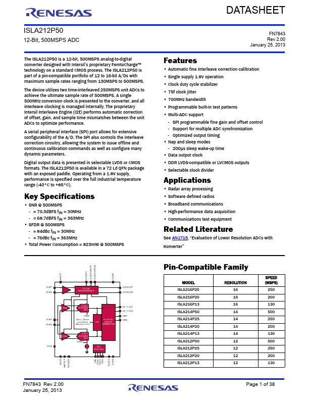
ISLA212P50 12-Bit, 500MSPS ADC The ISLA212P50 is a 12-bit, 500MSPS analog-to-digital converter designed with Intersil’s proprietary FemtoCharge™ technology on a standard CMOS process. The ISLA212P50 is part of a pin-compatible portfolio of 12 to 16-bit A/Ds with maximum sample rates ranging from 130MSPS to 500MSPS. The device utilizes two time-interleaved 250MSPS unit ADCs to achieve the ultimate sample rate of 500MSPS. A single 500MHz conversion clock is presented to the converter, and all interleave clocking is managed internally. The proprietary Intersil Interleave Engine (I2E) performs automatic correction of offset, gain, and sample time mismatches between the unit ADCs to optimize performance. A serial peripheral interface (SPI) port allows for extensive configurability of the A/D.
Published: |