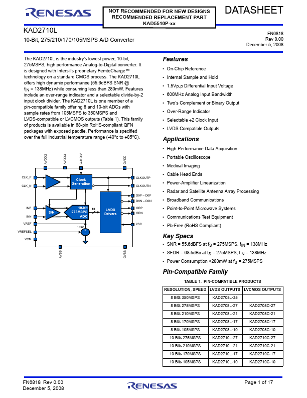
7
Pinout 8
Typical Performance Curves 9
Functional Description 12 Reset 12 Voltage Reference 12 Analog Input 12 Clock Input 13 Jitter 13 Digital Outputs 14
Equivalent Circuits 14
Layout Considerations 15 Split Ground and Power Planes 15 Clock Input Considerations 15 Bypass and Filtering
Key Features
include an over-range indicator and a selectable divide-by-2 input clock divider. The KAD2710L is one member of a pin-compatible family offering 8 and 10-bit ADCs with sample rates from 105MSPS to 350MSPS and LVDS-compatible or LVCMOS outputs (Table 1). This family of products is available in 68-pin RoHS-compliant QFN packages with exposed paddle. Performance is specified over the full industrial temperature range (-40°c to +85°C). AVDD2 AVDD3 CLKDIV OVDD
CLK_P CLK_N
Clock Generation
INP INN.
Full PDF Text Transcription for KAD2710L (Reference)
Note: Below is a high-fidelity text extraction (approx. 800 characters) for
KAD2710L. For precise diagrams, and layout, please refer to the original PDF.
KAD2710L NOT RECOMMENDED FOR NEW DESIGNS RECOMMENDED REPLACEMENT PART KAD5510P-xx 10-Bit, 275/210/170/105MSPS A/D Converter DATASHEET FN6818 Rev 0.00 December 5, 2008 AVS...
View more extracted text
0/105MSPS A/D Converter DATASHEET FN6818 Rev 0.00 December 5, 2008 AVSS OVSS The KAD2710L is the industry’s lowest power, 10-bit, 275MSPS, high performance Analog-to-Digital converter. It is designed with Intersil’s proprietary FemtoCharge™ technology on a standard CMOS process. The KAD2710L offers high dynamic performance (55.6dBFS SNR @ fIN = 138MHz) while consuming less than 280mW. Features include an over-range indicator and a selectable divide-by-2 input clock divider. The KAD2710L is one member of a pin-compatible family offering 8 and 10-bit ADCs with sample rates from 105MSPS to 350MSPS and LVDS-compatible or LVCMO