Datasheet4U Logo Datasheet4U.com
Renesas logo

MPC9447 Datasheet

Manufacturer: Renesas
MPC9447 datasheet preview

MPC9447 Details

Part number MPC9447
Datasheet MPC9447 Datasheet PDF (Download)
File Size 291.98 KB
Manufacturer Renesas
Description LVCMOS Clock Fanout Buffer
MPC9447 page 2 MPC9447 page 3

MPC9447 Overview

MPC9447 is specifically designed to distribute LVCMOS patible clock signals up to a frequency of 350 MHz. Each output provides a precise copy of the input signal with a near zero skew. The outputs buffers support driving of 50  terminated transmission lines on the incident edge.

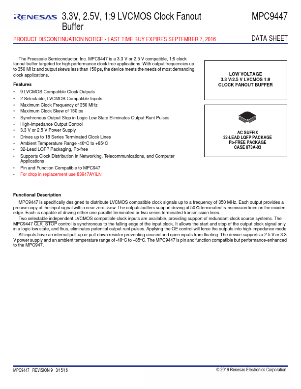
MPC9447 Key Features

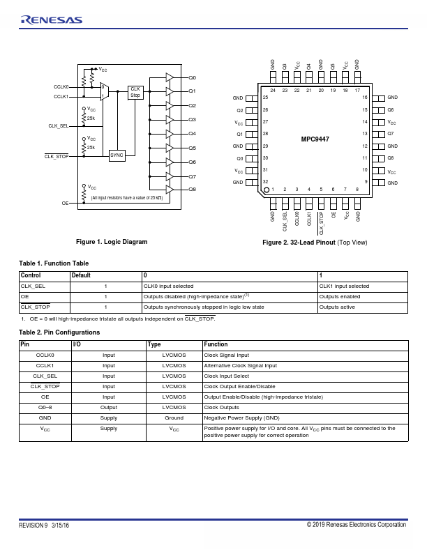
  • 9 LVCMOS patible Clock Outputs
  • 2 Selectable, LVCMOS patible Inputs
  • Maximum Clock Frequency of 350 MHz
  • Maximum Clock Skew of 150 ps
  • Synchronous Output Stop in Logic Low State Eliminates Output Runt Pulses
  • High-Impedance Output Control
  • 3.3 V or 2.5 V Power Supply
  • Drives up to 18 Series Terminated Clock Lines
  • Ambient Temperature Range -40C to +85C
  • 32-Lead LQFP Packaging, Pb-free

Similar Datasheets

Brand Logo Part Number Description Manufacturer
Motorola Logo MPC9447 3.3V/2.5V 1:9 LVCMOS Clock Fanout Buffer Motorola
IDT Logo MPC9447 3.3V/2.5V 1:9 LVCMOS Clock Fanout Buffer IDT

MPC9447 Distributor

More datasheets by Renesas

See all Renesas parts

Datasheet4U Logo
Since 2006. D4U Semicon. About Datasheet4U Contact Us Privacy Policy Purchase of parts