Datasheet4U Logo Datasheet4U.com
Renesas logo

MPC9824 Datasheet

Manufacturer: Renesas
MPC9824 datasheet preview

Datasheet Details

Part number MPC9824
Datasheet MPC9824-Renesas.pdf
File Size 420.76 KB
Manufacturer Renesas
Description Clock Generator
MPC9824 page 2 MPC9824 page 3

MPC9824 Overview

The MPC9824 uses a PLL with a 25 MHz input reference frequency to generate a single bank of 6 configurable LVCMOS output clocks. The output frequency of this bank is configurable by three FSEL pins. The 25 MHz reference may be either an external frequency source or a 25 MHz crystal.

MPC9824 Key Features

  • 6 LVCMOS outputs for processor and other system circuitry
  • 3 Buffered 25 MHz reference clock outputs
  • Crystal oscillator or external reference input
  • 25 MHz Input reference frequency
  • Selectable output frequencies = 33.33, 50, 66.66, 100, 125, 133.33, 166.66
  • Low cycle-to-cycle and period jitter
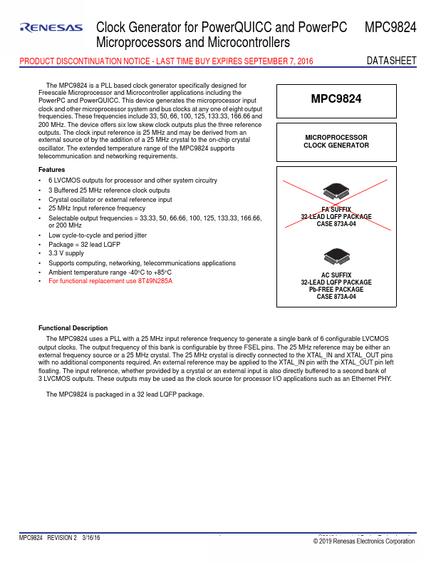
  • Package = 32 lead LQFP
  • 3.3 V supply
  • Supports puting, networking, telemunications

MPC9824 Applications

  • 6 LVCMOS outputs for processor and other system circuitry
Renesas logo - Manufacturer

More Datasheets from Renesas

See all Renesas datasheets

Part Number Description
MPC9893 3.3V 1:12 LVCMOS PLL Clock Generator
MPC940L LOW VOLTAGE 1:18 CLOCK DISTRIBUTION CHIP
MPC9446 LVCMOS Clock Fanout Buffer
MPC9447 LVCMOS Clock Fanout Buffer
MPC94551 Low Voltage 1:4 CMOS Clock Buffer
MPC962305 3.3V Zero Delay Buffer
MPC9772 3.3V 1:12 LVCMOS PLL Clock Generator
MPC9773 LVCMOS PLL Clock Generator

MPC9824 Distributor

Datasheet4U Logo
Since 2006. D4U Semicon. About Datasheet4U Contact Us Privacy Policy Purchase of parts