RC19104
RC19104 is PCIe Gen7 1.8V Fanout Buffer manufactured by Renesas.
- Part of the RC19108 comparator family.
- Part of the RC19108 comparator family.
features
, easing system design. They can drive both sourceterminated and double-terminated loads, operating up to 400MHz.
The family offers 2, 4, or 8 Low-Power (LP) HCSL output pairs in 3 × 3, 4 × 4, and 5 × 5 mm packages. The RC191xx devices offer higher output counts in smaller packages pared to earlier buffer families. The buffers support both mon Clock (CC) and Independent Reference (IR) PCIe clock architectures.
Applications
- Cloud/High-performance puting
- n VME storage
- Networking
- AI Accelerators
Features
- PCIe Gen5 additive phase jitter: 5.9fs RMS
- PCIe Gen6 additive phase jitter: 3.5fs RMS
- PCIe Gen7 additive phase jitter: 2.4fs RMS
- DB2000Q additive phase jitter: 10fs RMS
- 12k Hz to 20MHz additive phase jitter: 33fs RMS at
156.25MHz
- Power Down Tolerant (PDT) inputs
- Flexible Startup Sequencing (FSS)
- Automatic Clock Parking (ACP) upon loss of CLKIN
- Spread-spectrum tolerant
- CLKIN accepts HCSL or LVDS signal levels
- -40 to +105°C, 1.8V ± 5% operation
- Devices provide:
- Pin or SMBus selectable 33Ω, 85Ω, or 100Ω differential output impedance
- Pin or SMBus selectable output slew rate
- Pin or SMBus selectable output amplitude
- 9 SMBus addresses plus write protection
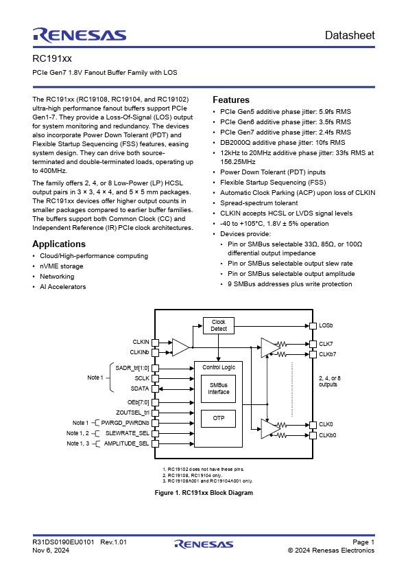
CLKIN CLKINb
Note 1
SADR_tri[1:0] SCLK
SDATA
Note 1 Note 1, 2 Note 1, 3
OEb[7:0] ZOUTSEL_tri PWRGD_PWRDNb SLEWRATE_SEL AMPLITUDE_SEL
Clock Detect
Control Logic SMBus Interface
1. RC19102 d oes not have these pin s. 2. RC19108, RC1 9104 only. 3. RC19108A001 and RC19104A001 only.
Figure 1. RC191xx Block Diagram
LOSb CLK7 CLKb7
2, 4, or 8 outputs
CLK0...