Datasheet Summary
Dual Schmitt-trigger Buffers
REJ03D0757- 0100 Rev.1.00
Jul 26, 2006
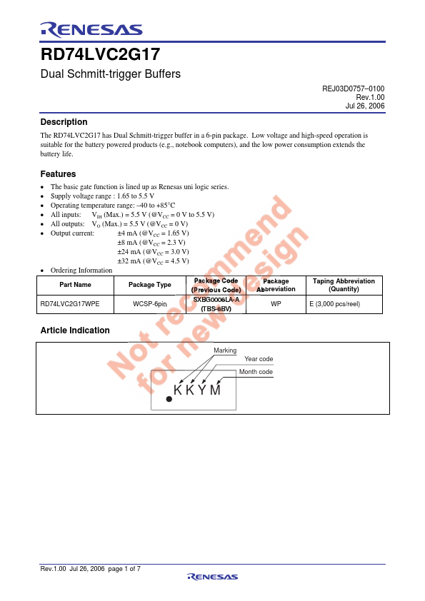
Description
The RD74LVC2G17 has Dual Schmitt-trigger buffer in a 6-pin package. Low voltage and high-speed operation is suitable for the battery powered products (e.g., notebook puters), and the low power consumption extends the battery life.
Features
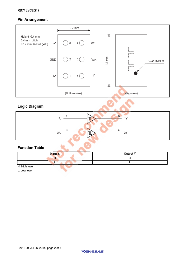
- The basic gate function is lined up as Renesas uni logic series.
- Supply voltage range : 1.65 to 5.5 V
- Operating temperature range:
- 40 to +85°C
- All inputs: VIH (Max.) = 5.5 V (@VCC = 0 V to 5.5 V)
- All outputs: VO (Max.) = 5.5 V (@VCC = 0 V)
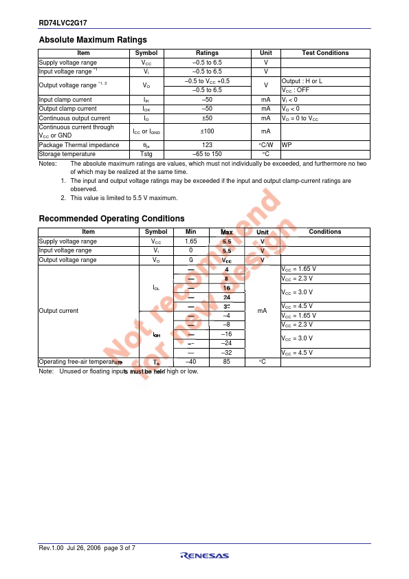
- Output current:
±4 mA (@VCC = 1.65 V)
±8 mA (@VCC = 2.3 V)
±24 mA (@VCC = 3.0 V)
±32 mA (@VCC = 4.5...