Datasheet4U Logo Datasheet4U.com

RNA52A10TH5 - Dual CMOS system-RESET

This page provides the datasheet information for the RNA52A10TH5, a member of the RNA52A10T Dual CMOS system-RESET family.

Datasheet Summary

Description

The RNA52A10T incorporates two reset circuits, one with and one without a delay function, allowing the generation of separate reset signals for a microprocessor and associated system circuits.

Features

  • Two CMOS reset circuits, one with and one without the delay function.
  • Reference voltage: 1.0 V.
  • Reference voltage accuracy: ± 50 mV.
  • Reference voltage hysteresis: 6% (typ. ).
  • Low current consumption: 1.1 μA (typ. ).
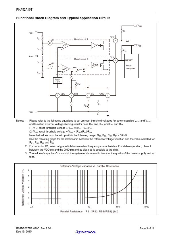
  • Delay time set by an external CR circuit.
  • Manual reset input.
  • Open-drain output.
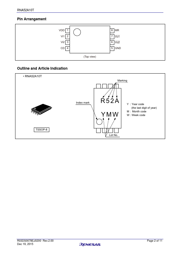
  • TSSOP-8 (8-pin) package.
  • Operating temperature range:.
  • 40 to 85°C.
  • Ordering Information Part Na.

📥 Download Datasheet

Datasheet preview – RNA52A10TH5

Datasheet Details

Part number RNA52A10TH5
Manufacturer Renesas
File Size 281.06 KB
Description Dual CMOS system-RESET
Datasheet download datasheet RNA52A10TH5 Datasheet
Additional preview pages of the RNA52A10TH5 datasheet.
Other Datasheets by Renesas

Full PDF Text Transcription

Click to expand full text
Data Sheet RNA52A10T Dual CMOS system–RESET IC R03DS0078EJ0200 Rev.2.00 Dec 19, 2015 Description The RNA52A10T incorporates two reset circuits, one with and one without a delay function, allowing the generation of separate reset signals for a microprocessor and associated system circuits. The detection voltage of each reset circuit is determined by the value of an external resistor, and the internal reference voltage is 1.0 V. The CMOS process for the RNA52A10T means that the device draws only 1.1 μA (typ.). The reset cancellation delay time is set with a high degree of accuracy by the values of a capacitor and resistor connected with the CD pin.
Published: |