SLG59M1599V Overview
Key Specifications
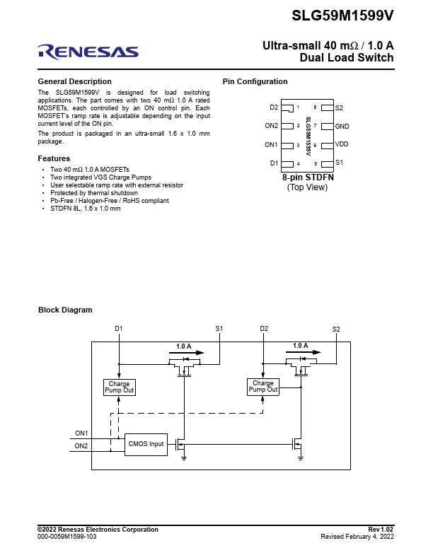
Pins: 8
Operating Voltage: 5 V
Max Voltage (typical range): 5.5 V
Min Voltage (typical range): 2.5 V
Description
The SLG59M1599V is designed for load switching applications. The part comes with two 40 mΩ 1.0 A rated MOSFETs, each controlled by an ON control pin.
Key Features
- Two 40 mΩ 1.0 A MOSFETs
- Two integrated VGS Charge Pumps
- User selectable ramp rate with external resistor
- Protected by thermal shutdown
- Pb-Free / Halogen-Free / RoHS compliant