SLG7NT4375
Overview
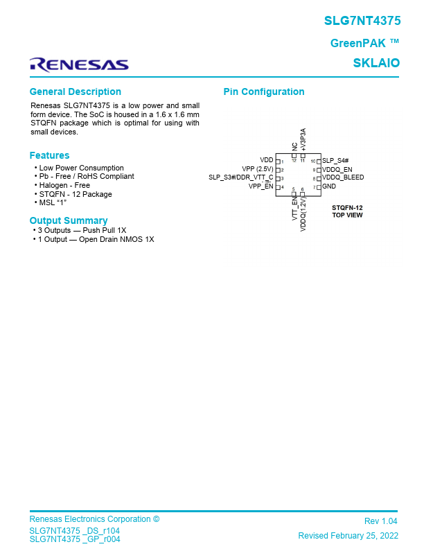
Renesas SLG7NT4375 is a low power and small form device. The SoC is housed in a 1.6 x 1.6 mm STQFN package which is optimal for using with small devices.
- Low Power Consumption
- Pb - Free / RoHS Compliant
- Halogen - Free
- STQFN - 12 Package
- MSL “1” Output Summary
- 3 Outputs - Push Pull 1X
- 1 Output - Open Drain NMOS 1X VDD VPP (2.5V) SLP_S3#/DDR_VTT_C VPP_NETNL SLP_S4# VDDQ_EN VDDQ_BLEED GND VTT_EN VDDQ(1.2V) Renesas Electronics Corporation ©