UPD70F3737 Description
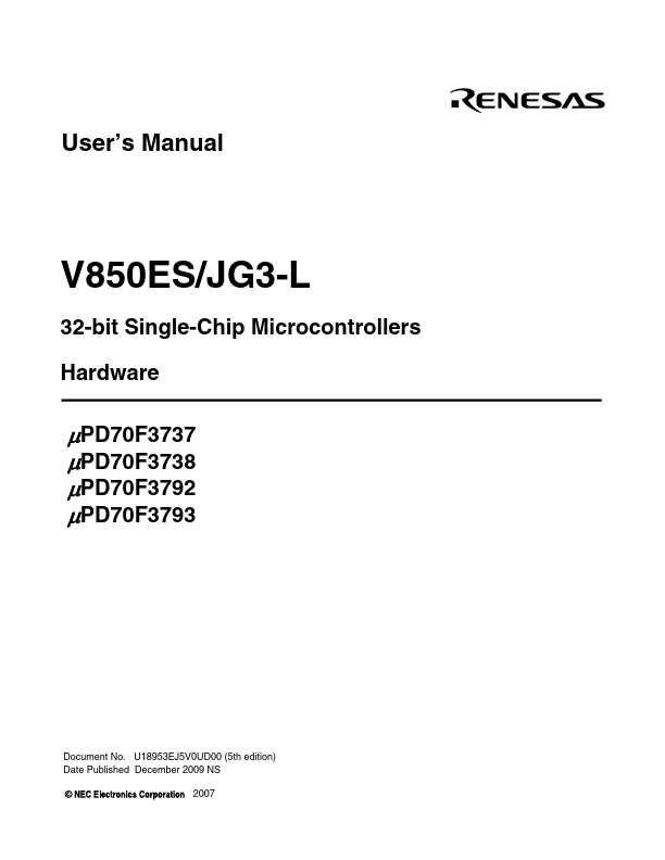
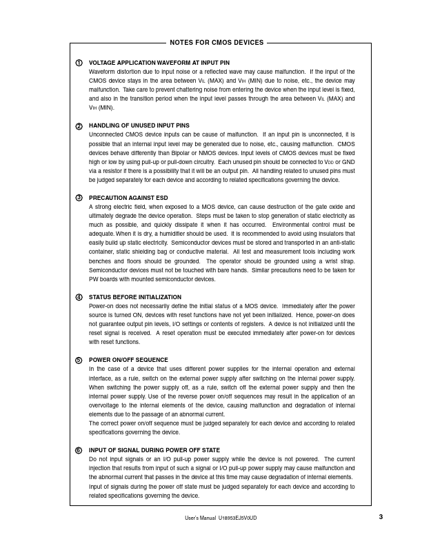
User’s Manual V850ES/JG3-L 32-bit Single-Chip Microcontrollers Hardware μPD70F3737 μPD70F3738 μPD70F3792 μPD70F3793 Document No. If the input of the CMOS device stays in the area between VIL (MAX) and VIH (MIN) due to noise, etc., the device may malfunction. Take care to prevent chattering noise from entering the device when the input level is fixed, and also in the transition period when the input level passes...


