X28HC64
features the JEDEC approved pinout for byte-wide memories, patible with industry standard RAMs.
The X28HC64 supports a 64-byte page write operation, effectively providing a 32µs/byte write cycle, and enabling the entire memory to be typically written in 0.25 seconds. The X28HC64 also features
DATA Polling and Toggle Bit Polling, two methods providing early end of write detection. In addition, the X28HC64 includes a user-optional software data protection mode that further enhances Intersil’s hardware write protect capability.
Intersil EEPROMs are designed and tested for applications requiring extended endurance. Inherent data retention is greater than 100 years.
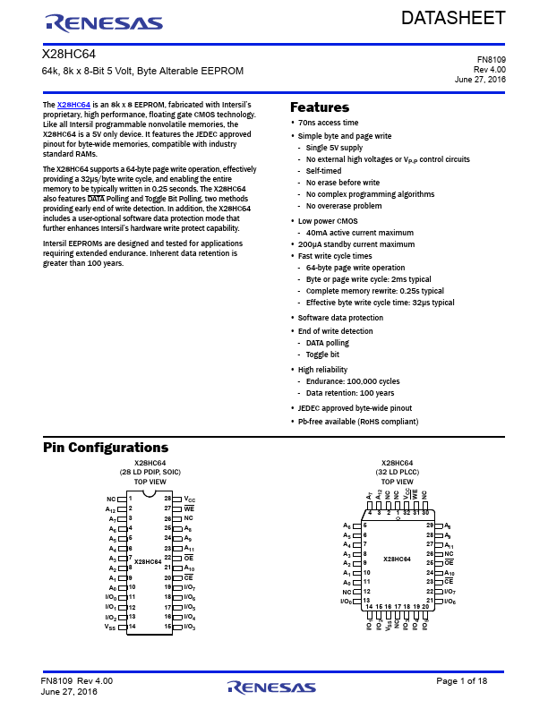
Pin Configurations
X28HC64 (28 LD PDIP, SOIC)
TOP VIEW
A12 A7 A6 A5 A4 A3 A2 A1 A0
I/O0 I/O1
I/O2 VSS
1 28 2 27 3 26 4 25 5 24 6 23 7 X28HC64 22 8 21 9 20 10 19 11 18 12 17 13 16 14 15
VCC WE NC
A8 A9 A11 OE A10 CE I/O7 I/O6 I/O5 I/O4 I/O3
FN8109 Rev 4.00 June 27, 2016
Features
- 70ns access time
- Simple...