BU2185F
BU2185F is Clock generator manufactured by ROHM.
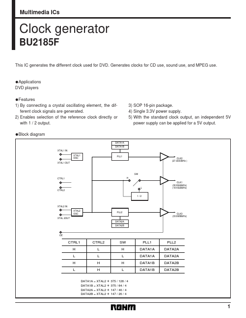
Features
- 1) By connecting a crystal oscillating element, the different clock signals are generated. 2) Enables selection of the reference clock directly or with 1 / 2 output.
3) SOP 16-pin package. 4) Single 3.3V power supply. 5) With the standard clock output, an independent 5V power supply can be applied for a 5V output.
- Block diagram
DATA1A DATA1B XTAL1 IN XTAL1 OSC XTAL1 OUT PLL1 CLK2 (27.0000MHz )
SW CTRL1 H CLK1 (36.8640MHz) (18.4320MHz)
L CTRL2 1/2
XTAL2 IN XTAL2 OSC XTAL 2OUT DATA2A DATA2B PLL2 CLK3 (33.8688MHz)
CTRL1 H L H L
CTRL2 L L H H
DATA1A = XTAL2 ∗ DATA1B = XTAL2 ∗ DATA2A = XTAL2 ∗ DATA2B = XTAL2 ∗
SW H L H L
375 / 128 / 4 375 / 64 / 4 147 / 40 / 4 147 / 20 / 4
PLL1 DATA1A DATA1A DATA1B DATA1B
PLL2 DATA2A DATA2A DATA2B DATA2B
Multimedia ICs
- Absolute maximum ratings (Ta = 25°C)
Parameter Applied voltage Input voltage Power dissipation Storage temperature Symbol VDD VIN Pd Tstg Limits
- 0.5 ~ + 7.0
- 0.5 ~ VDD + 0.5 450∗
- 30 ~ + 125 Unit V V m W °C
᭺Does not represent guaranteed performance. ∗ Reduced by 4.5m W for increase in Ta of 1°C over 25°C. ᭺Not designed for radiation resistance.
- Remended operating conditions (Ta = 25°C)
Parameter Power supply voltage Input high level voltage Input low level voltage Operating temperature Output load Symbol VDD VIH VIL Topr CL Limits 3.0 ~ 3.6 0.8 × VDD ~ VDD 0.0 ~ 0.2 × VDD
- 5 ~ + 70 15 (Max.) Unit V V V °C p F
- Pin descriptions
Pin No. 1 2 3 4 5 6 7 8 9 10 11 12 13 14 15 16 Pin name XTAL1-IN XTAL1-OUT CTRL2 AGND DGND DVDD XTAL2-IN XTAL2-OUT CLK1 DVDD CLK2 DVDD AVDD CLK3 CTRL1 OE Pin descriptions Reference oscillation input 1 (not used) Reference oscillation output 1 XTAL setting (Low: XTAL = 36.8MHz mode; High: XTAL = 18.4MHz mode) Analog GND Digital GND Independent power supply for XTAL2-IN and XTAL2-OUT pins Reference oscillation input 2 (36.864MHz or 18.432MHz) Reference oscillation output 2 Reference clock output (36.864MHz or 18.432MHz) Independent power supply for CLK1...