Datasheet4U Logo Datasheet4U.com

BU4081BFV - Quad 2-input AND gate

Key Features

  • 1) Low power dissipation. 2) Wide range of operating power supply voltages. 3) High input impedance. 4) High fan-out. 5) Direct drive of 2 L-TTL inputs and 1 LS-TTL input.
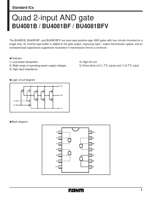
  • Logic circuit diagram VDD OUT IN IN VSS.
  • Block diagram A1 1 14 VDD 13 A4 12 B4 11 O4 10 O3 9 B1 2 O1 3 O2 4 B2 5 A2 6 B3 VSS 7 8 A3 1 Standard ICs BU4081B / BU4081BF / BU4081BFV SS.
  • Absolute maximum ratings (Ta = 25°C,V Parameter Power supply voltage Power dissipation Oper.

📥 Download Datasheet

Datasheet Details

Part number BU4081BFV
Manufacturer ROHM
File Size 50.07 KB
Description Quad 2-input AND gate
Datasheet download datasheet BU4081BFV Datasheet

Full PDF Text Transcription (Reference)

The following content is an automatically extracted verbatim text from the original manufacturer datasheet and is provided for reference purposes only.

View original datasheet text
Standard ICs Quad 2-input AND gate BU4081B / BU4081BF / BU4081BFV The BU4081B, BU4081BF, and BU4081BFV are dual-input positive-logic AND gates with four circuits mounted on a single chip. An inverter-type buffer is added to the gate output, improving input / output transmission speed, and an increased load capacitance suppresses fluctuation in transmission time to a minimum. Features • 1) Low power dissipation. 2) Wide range of operating power supply voltages. 3) High input impedance. 4) High fan-out. 5) Direct drive of 2 L-TTL inputs and 1 LS-TTL input.