Description
Pin name
OSC1 OSC2 V1 ~ V3 VSS VDD SCK
SD
9
I
CS
10
I
C/D COM0
11
I
12 ~ 15 COM3 RESET SEG0 17 ~ 48 SEG31 16
O
I
O
Input / output equivalent circuits
Pin name I / O SD SCK C/D CS I
VDD IN GND
Equivalent Circuit
Pin name I / O SEG0 SEG31
OUT
Equivalent Circuit
VLCD
O
~
Features
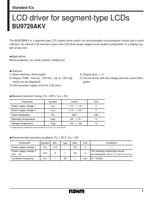
- 1) Serial interface. (8-bit length) 2) Display RAM: Internal, 128 bits. (up to 128 segments can be displayed) 3) Internal power supply circuit for LCD drive. 4) Display duty: 1 / 4 5) Can be driven with low voltage and low current dissipation.
- Absolute maximum ratings (Ta = 25°C, V
Parameter
Power supply voltage 1 Power supply voltage 2 Power dissipation Operating temperature Storage temperature
SS
= 0V)
Limits.
- 0.3 ~ + 7.0.
- 0.3 ~ + VDD 400∗.
- 20.